RF, Digital Radio and
Metamaterial Fundamentals
Project
Digital Non-Foster Circuits and Non-Foster Antennas
Overview
Work in assigned project groups.
The objective of this project is to simulate Project: Digital NonFoster Circuits and Non-Foster Antennas.
NOTE: Use the Project Report Template and keep answers to questions on consecutive sheets
of paper with all plots at the end.
IN NO CASE may code or files be exchanged between students, and
each student must answer the questions themselves and do their own
plots, NO COPYING of any sort! Nevertheless, students are
encouraged to collaborate in the lab session.
Part 1: Digital Non-Foster Circuit Simulation
- In this part, we investigate Project: Digital NonFoster Circuits for negative capacitance
- This used in Digital Non-Foster Radio Architectures for wideband matching of electrically small antennas
- For details on radio design concepts, see:
- Load and run the Maathcad digital non-Foster simulation file as follows:
- Download file rfDigRadMeta18zTxNonFos_a.xmcd.zip
and unzip it
to your preferred Maathcad directory/folder
- Run Maathcad program, and open the "rfDigRadMeta18zTxNonFos_a.xmcd" design,
- You MUST edit the Maathcad file to obtain the proper plot for your report
- Near the bottom of the file, it computes the digital non-Foster input impedance Zin(s) as
- You should see these formulas near the bottom of the rfDigRadMeta18zTxNonFos_a.xmcd Maathcad file
See the following paper containing the theory and needed parameters:
Near the bottom of the file, you will see the plot that must be added to your report
It has errors, and will look similatr to this:
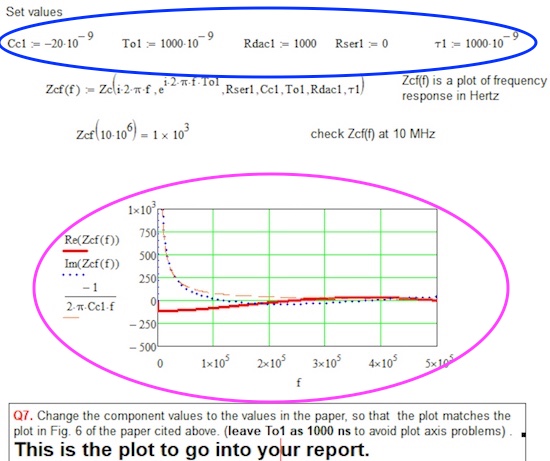
Fig 001
At what frequency does the imaginary part of Zin(s) begin to diverge from the ideal reactance of a negative capacitor?
What is the sample rate of the system?
As an optional exercise, reduce latency to 1 ns, and observe the changes
s
What clock determines the carrier frequency?
Save your work!
Part 2: Non-Foster Antenna Bandwidth Improvement
From a Linux terminal, ADS should be available in the
menu (Applications::ElecEngineering::KeysightAdvancedDesignSystem)
- From a PC terminal, you must first open a remote Linux
session,
then proceed as for a Linux terminal
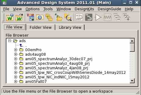
- After ADS starts you should get a starting window similar to
this (navigate into your apps/ads folder):
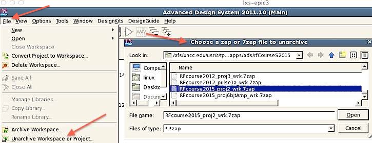
- Load and run the pulse example as follows:
- Download the 7zap
archive as follows:
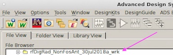
- You should find a new directory rrfDigRad_NonFosAnt_30jul2018a_wrk
created in apps/ads
- Run ADS and open the new RFcourse2012_pulse1a_wrk workbook
by double-clicking it
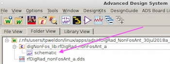
- Go down through the directory tree to pulse1/schematic and
double click that schematic file
- and the following schematic
should appear.
- The circuit in the cyan circle below takes s-parameters of the antenna (Zant, S33)
- The circuit in the yellow circle below takes s-parameters of the passively-matched (inductor-matched) antenna (ZindMatch, S22)
- The circuit in the blue circle below takes s-parameters of the non-Foster (-40pF) matched antenna (ZnonFos, S11)
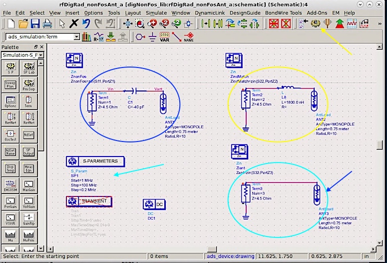
Fig 002
- Double-click the transmission antenna (blue arrow above) and look at the variables
in the pop-up menu.
- Use the mouse to select the variables and observe the
changing description at the bottom of the pop-up.
- Double-click the "gear" icon (yellow arrow above) in the upper
right of the window to simulate.
- After simulation the plotted results should pop up in a new window
- One plot is the s-parameters similar to below
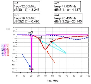
FIg 003
- The dip in S22 (blue arrow above) it the center frequency of the passive match at 20 MHz
- Adjust your non-Foster capacitor (-40 pF originally) so that the dip in S12 (red arrow above) is also at 20 MHz
- Then, slide markers m1 and m2 to measure the bandwidth at the -6 dB points
- Save this new plot for your report
- Record the 2 frequencies and bandwidth for your report
- Record the new value for your non-Foster capacitance (changed from the original -40 pf)
- Then, slide markers m3 and m4 to measure the passive-matched antenna bandwidth at the -6 dB points
- Record the 2 frequencies and bandwidth for your report
- Rerun the simulation one last time to make sure that your plot is for the final value of the capacitor
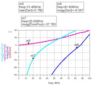
- The second plot is the impedance, similar to below
Fig 004
- Use your adjusted new value from above for your non-Foster capacitor (-40 pF originally)
- Save this new plot for your report
- Then, slide marker m5 to 20MHz to measure the real part of the antenna Zant at the tuned frequency
- Then, slide marker m7 to 20MHz to measure the imaginary part
of the non-Foster matched antenna ZnonFos at the tuned frequency (it
should be near zero ohms!)
- Record the measured values for your report
- See report template below
Report Data
- ============================
WARNING !! ====================================
- **** WARNING **** YOU MUST USE
THE PROJECT REPORT TEMPLATE Below:
- See the Project
Report Template at bottom of this page
- A well-written report/paper is
EXPECTED
- STRONGLY RECOMMEND that you read IEEE
authorship series: How to Write for Technical Periodicals
& Conferences
- Clearly describe everything, including:
- variables in block diagrams
- variables in formulas
- units of variables kHz, pF, nH, m, s,
- all traces on plots
- all curves on plots
- all results in any tables
- Minimum required data content for
your report and demos
- Required theory/formulas numbered as below:
- (1) formula for Zin(s) as shown above
- (2) formula for Hrc(z) as shown above
- Required figures:
- Any illegible plots receive zero credit (must be able to read all numbers, axes, labels, curves, grids, titles, legends)
- All plots must of professional quality as in IEEE papers
- LEGIBLE block diagram of the Thevenin digital non-Foster circuit that you simulated (see the circuit in the paper)
- LEGIBLE simulation showing Zin(s) as in Fig 001 above (magenta circle), with appropriate caption
- LEGIBLE schematic showing the non-Foster antenna match circuit as in Fig 002 (blue circle only)
- LEGIBLE simulation showing s-parameters including your final non-Foster match as in Fig 003
- LEGIBLEsimulation showing impedances including your final non-Foster match as in Fig 004
- Required tabular data content:
- Table of Maathcad results with 4 columns: frequency in kHz, Maathcad imaginary part of Zin(s), and ideal reactance, and percent error from ideal
- Row 1: imaginary part of Zin(s), and ideal reactance at 50 kHz
- Row 2: imaginary part of Zin(s), and ideal reactance at 100 kHz
- Row 3: imaginary part of Zin(s), and ideal reactance at 150 kHz
- Table of ADS results with 2 columns: parameter and parameter value
- Row 1: the final value of your non-Foster capacitance (change to the -40 pf) in pF
- Row 2: the final bandwidth of your non-Foster match in MHz
- Row 3: the bandwidth of the passive match in MHz
- Row 4: the real part of the antenna Zant at 20 MHz
- Row 4: the imaginary part of your non-Foster matched antenna ZnonFos at 20 MHz
See report template below
NOTE ReportTemplate: Use the Project Report Template
YOU MUST ADD CAPTIONS AND FIGURE
NUMBERS TO ALL FIGURES!!
Copyright © 2010-2018 T. Weldon
ANSYS, and HFSS are registered trademarks of ANSYS, Inc.
Cadence, Spectre and Virtuoso are registered trademarks of
Cadence Design Systems, Inc., 2655 Seely Avenue, San Jose, CA
95134. Keysight is a registered trademarks of Keysight
Technologies, Inc. MATLAB and Simulink are registered
trademarks of The MathWorks, Inc. MATHCAD is a trademark of PTC INC.