f
Radio Frequency Design Project 7
Overview
Remain in same project groups for the
semester.
The objective of this project is to work with couplers
NOTE: Use the Project
Report
Template and keep answers to
questions on consecutive sheets of paper with all plots at the
end.
IN NO CASE may code or files be exchanged between students, and
each student must answer the questions themselves and do their own
plots, NO COPYING of any sort! Nevertheless, students are
encouraged to collaborate in the lab session.
Only turn in requested plots ( Pxx )
and requested answers to questions ( Qxx ).
Part 1
Part 2
- Next, automatically layout your branch line coupler design.
Part 3
- Download the p7_radio12.zip
cadence files, and use the p7_radio12 file password given by
the instructor.
- Extract the file and the sub-directory zip file until you
recover the rfproj7 directory, and copy this into your
~/cadence6/NCSU16 directory
- Add this new library to your cds.lib file as before
- Run Cadence6 software
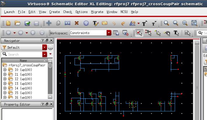
- Open the schematic of rfproj7_crossCoupPair as below:
- Plot the schematic ( P12 )
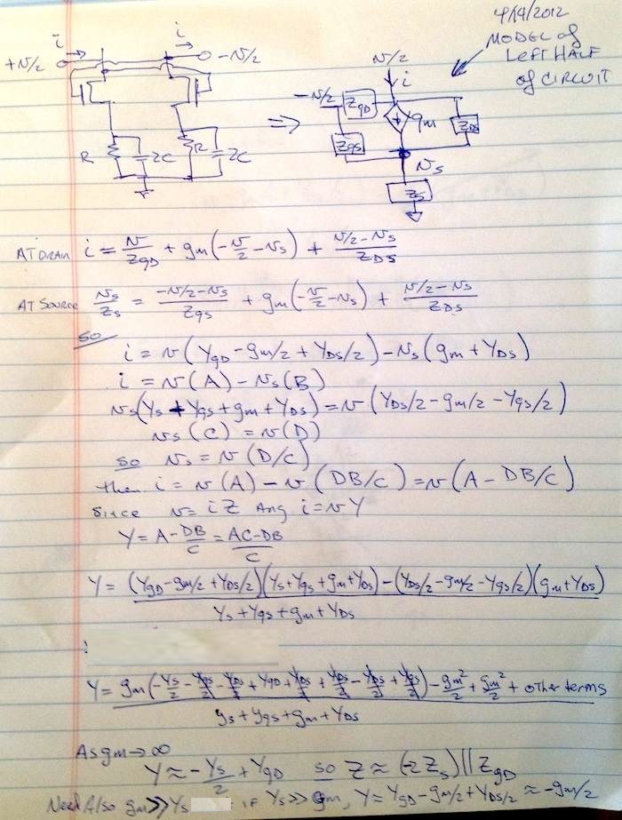
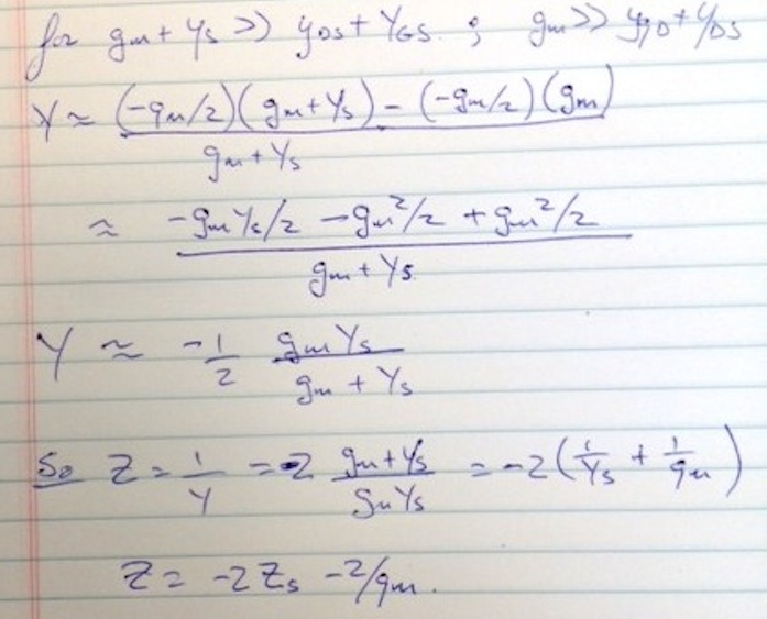
- The theory for the circuit is approximated from:
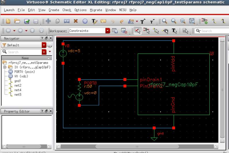
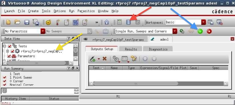
- Open the rfproj7_negCap10pF_testSparams schematic, as
illustrated below:
- Launch ADE XL using MenuBar::Launch::ADEXL and open the
existing view
- As before, run the simulation (blue arrow below)
- If you get an error regarding the model libraries such as:
- Unable to open input file
`/afs/uncc.edu/usr/r/tpweldon/linux/cadence6/ncsu_cdk_160_beta/models/spectre/nom/ami06N.m'
- Then,
- you must right-click the test (yellow arrow below) and
"OpenTestEditor"
- in the TestEditor run
MenuBar::Setup::ModelLibraries
- Delete the offending libraries
- As before, link to your own libraries
~/cadence6/ncsu_cdk_160_beta/models/spectre/nom/ami06N.m
and ami06P.m
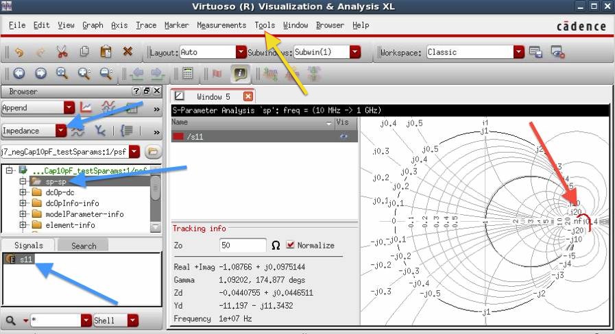
- Run the ResultsBrowser (red arrow above) to plot the results
- As shown below, plot the smith chart as before (blue arrows
below)
- Notice that the impedance is outside the normal region of
the Smith chart (red arrow above), indicating a negative
resistance in addition to any negative capacitance
- Plot the Smith chart ( P13 )
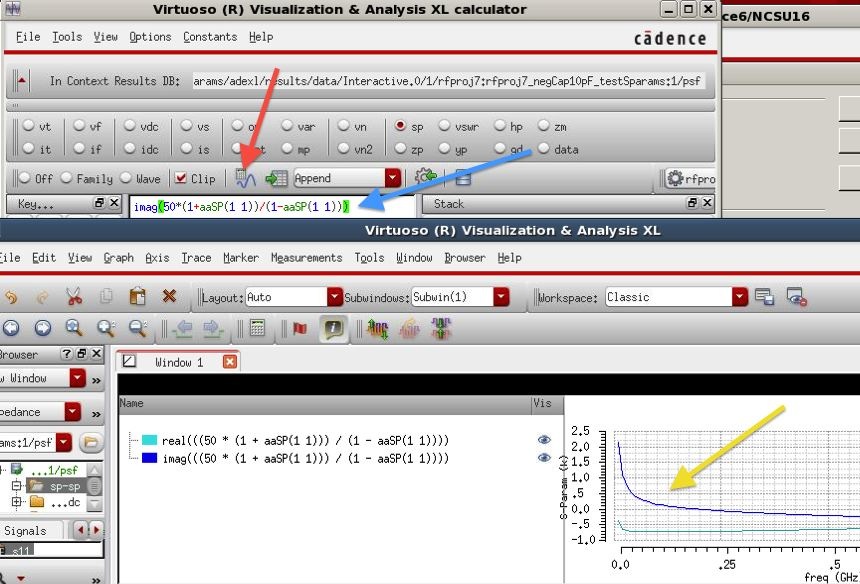
- Next, use the ResultsBrowser
MenuBar::Tools::Calculator (yellow arrow above) to create a
plot of the real and imaginary part of the impedance Z
- Enter the formula (blue arrow below) real(50*(1+aaSP(1
1))/(1-aaSP(1 1))) and click the Evaluate/Plot button (red
arrow below) :
- Enter the formula (blue arrow below) imag(50*(1+aaSP(1
1))/(1-aaSP(1 1))) and clicking the Evaluate/Plot button (red
arrow below) to append the new plot
- The final plot should appear as shown below (yellow arrow):
- Plot the real and imaginary part of the impedance (Change
the plot to a white background, and thick lines, one dashed
and one solid) ( P14 )
- Is the imaginary part of the impedance indicative of a
negative capacitance? ( Q7 )
- Is the real part of the impedance a negative
resistance at low frequency (~50 MHz)? (
Q8 )
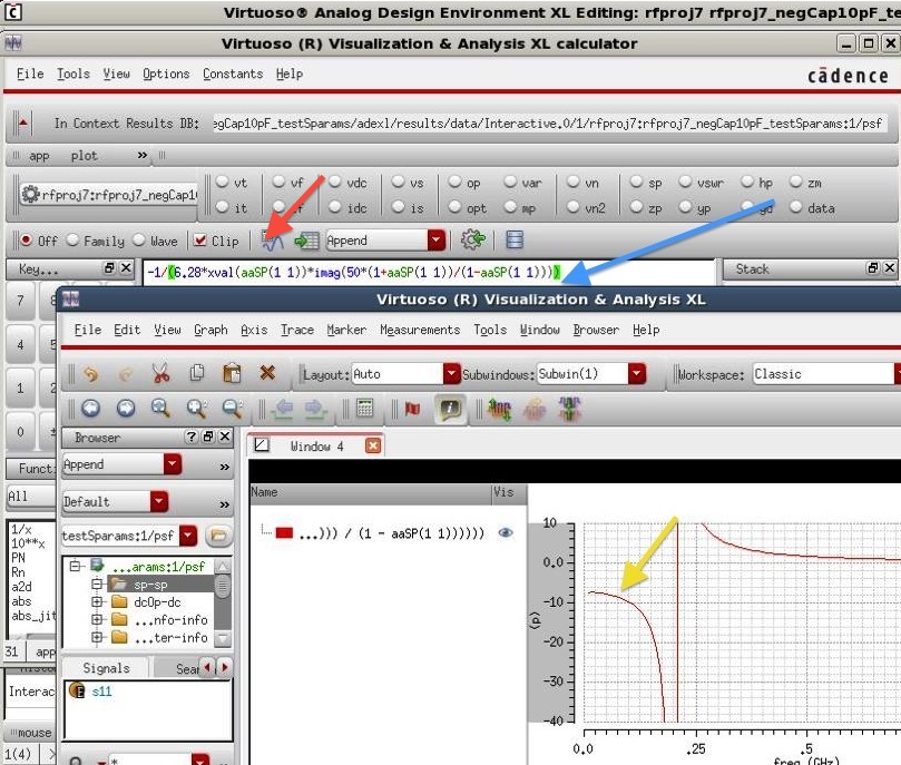
- Next, use the ResultsBrowser
MenuBar::Tools::Calculator to create a plot of the capacitance
associated with impedance Z
- Enter the formula (blue arrow below) -1/(6.28*xval(aaSP(1
1))*imag(50*(1+aaSP(1 1))/(1-aaSP(1 1)))) and click the
Evaluate/Plot button (red arrow below)
- The final plot, after resetting the scale from -40 pF to 10
pF, should appear as shown below (yellow arrow):
- Plot the capacitance as above (Change the plot to a white
background, and thick lines) ( P15
)
- What is the frequency range where the capacitance remains
within 10 percent of its value at the lowest frequency? ( Q9 )
- Finally, use a transient simulation to make sure that the
circuit is stable and does not oscillate
- Typically, the stable regions are roughly where both R and C
are negative, such that the poles remain in the stable Laplace
half-plane and the impulse response exp(-t/RC) remains
well-behaved.
- Open rfproj7_negCap10pF_testTrans schematic
- Launch ADE XL using MenuBar::Launch::ADEXL and open the
existing view
- As before, run the simulation (blue arrow below)
- Click PlotAllWaveforms button (red arrow below)
- The final plot should appear as shown below (yellow arrow):
- Plot the transient response as above (Change the plot to a
white background, and thick lines) ( P16 )
- Change the simulation duration to 2000 ns and re-plot the
transient response as above (Change the plot to a white
background, and thick lines) ( P17
)
- Is there any sign of instability or oscillation? ( Q10 )
Part 4
- Create a very simple layout, including padframe and ground pin
- Note: Pin 30 MUST ALWAYS BE GROUNDED
as described below
- In the rfproj7 directory, create a new cell schematic named
rfproj7_top
- This represents the "top" or highest level in your design
hierarchy
- Only use the word "top" in one cell
view in any future projects, so it can easily be found
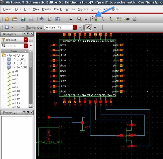
- Place the following instances (blue arrow below) on the
schematic
- a probe_gss_all from Library rfproj7,
- a padframe_1500 from from Library rfproj7,
- a wp100 from from Library rfproj7,
- and a "gnd" from Library analogLib/Sources/Globals
- probe_gss_all is a calibration circuit
for s-parameter measurement on chip, and must be added to
all designs
- Wire it as shown below, check and save the design (35
warnings for unused pins)
- Plot your schematic ( P18 )
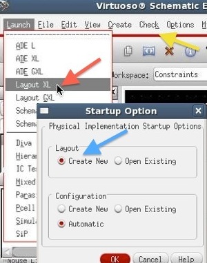
- As shown below, launch the Layout XL tool (red arrow
below)
- In the popup window, select create new (blue arrow below)
- In the Layout XL window, create a new layout using
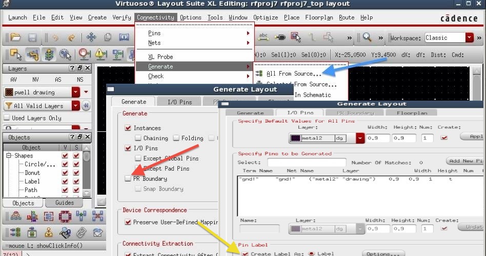
MenuBar::Connectivity::Generate::AllFromSource as below
- In the popup options windows, check the tabs for the options
(blue arrow below) and make sure PR boundary (place and route
boundary) is turned off as below (red arrow below)
- Make sure that the create label option is turned on (yellow
arrow below)
- Note that the "gnd!" pin from your schematic will be created
as metal1 0.9x0.9 micron pin
- As before in Layout XL, use MenuBar::Options::Display to set
the "Display Levels" to 0 to 30, and to set the check buttons
"on" for "Pin Names" and "Instance Pins."
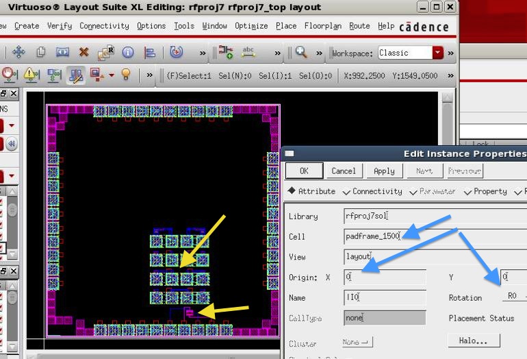
- Before doing anything else, select the padframe, type "q" on
the keyboard, and set the padframe at coordinates 0,0 (blue
arrows below)
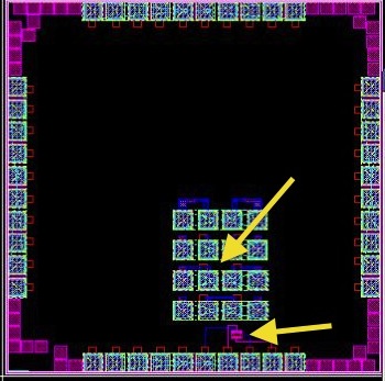
- Rearrange your layout as shown below
- Note: the very tiny "gnd!" pin will be hard to locate near
the 0,0 coordinate
- Place your probe_gss_all and wp100 as shown below (yellow
arrows below)
- Selecting a pin or device in the layout highlights the
corresponding item in the schematic
- Activate the annotation bowser pane using
MenuBar::Window::Assistants::AnnotationBrowser
- Then, use MenuBar::Connectivity::Nets::ShowAllIncompleteNets
to see the nets that must be connected
- You can move devices by typing "m" in the layout area
- Then, move your pins and devices into positions
approximately as below, where the nets will be easy to connect
and wire
- The cell for probe_gss_all must be
placed in an area where the probe will not bump into
wirebonds (top yellow arrow below)
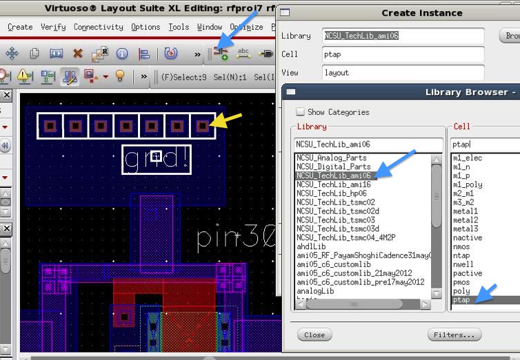
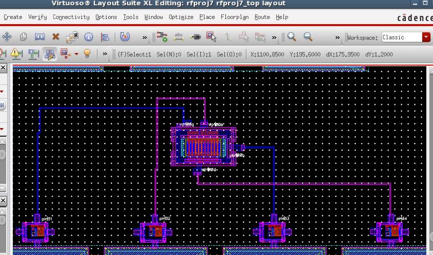
- Place your "gnd!" pin as below on pin 30
- Connect the gnd! pin to the substrate using metal1 (select
metal 1 in the palette and type "r" on the keyboard to draw a
metal1 rectangle)
- Then, add 7 "ptap" instances (yellow arrow below) in the
metal1 rectangle area as shown below, using the addInstance
button (blue arrows below)
- The ptaps connect the ground pin to the substrate, thereby
grounding the p-type substrate of the integrated circuit chip
- Always use pin 30 for ground, since it
has the shortest wirebonds with the lowest inductance
- The Pin 30 ground pin layout should appear as
illustrated below.
- Plot your Pin 30 layout as above ( P19 )
- Next, wire the transistor
- Select metal1 on the LayersPalette in the left side of the
Layout XL window, then type "p" on the keyboard when your
mouse is in the layout area to create a metal1
path. (Alternatively use
MenuBar::Create::Shape::Path)
- Connect your wp100 circuit as illustrated below using metal1
and/or metal 2 paths
- Experiment with typing "r" in the layout area to draw a
metal1 or metal2 rectangle
- Plot your wp100 layout as above (
P20 )
- Your final layout should appear as below:
- Plot your overall layout as above ( P21 )
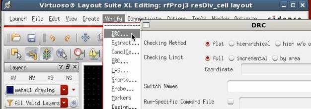
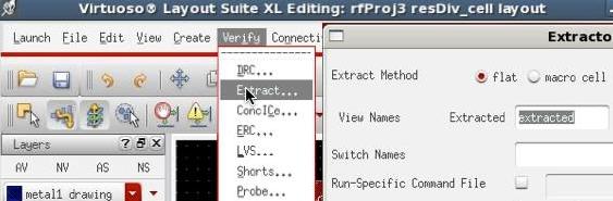
- Finally, perform DRC, Extraction, and LVS as before
- Run DRC as illustrated below
- Run Extraction as illustrated below
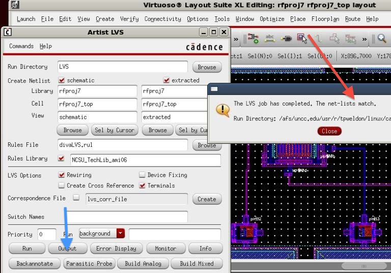
- Run LVS as illustrated below
- The netlists must match! (red
arrow below)
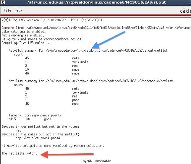
- Inspect the LVS output by pressing the output button (blue
arrow above)
- The output should appear as below
- Print your output as above and make sure to include your
home directory (blue arrow above) and netlists match (red
arrow above) ( P22 )
Report
NOTE: Use the
Project
Report
Template and
keep answers to
questions on consecutive sheets of paper with all plots at the
end.
Do not add extraneous pages or put
explanations on separate pages unless specifically directed to do
so. The instructor will not read extraneous pages!
Only turn in requested plots ( Pxx ) and requested answers to
questions ( Qxx ). All plots must be
labeled P1, P2, etc. and all questions must be numbered Q1, Q2,
etc. YOU MUST ADD CAPTIONS AND FIGURE NUMBERS TO ALL
FIGURES!!