Radio Frequency Design Project 5
Overview
Remain in same project groups for the
semester.
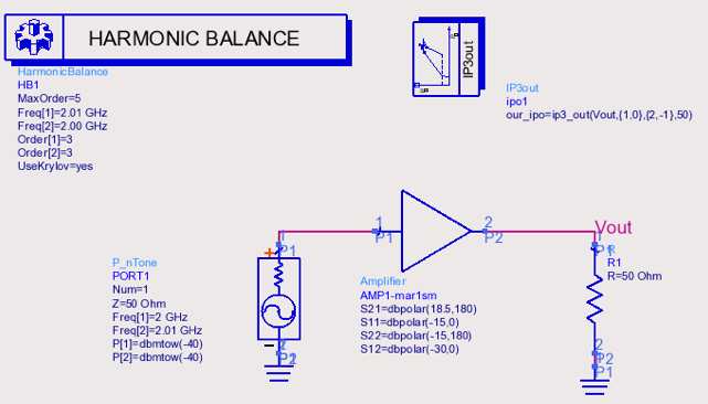
The objective of this project is to work with ADS harmonic balance,
cascade analysis, and HFSS
NOTE: Use the Project
Report Template and keep answers
to questions on consecutive sheets of paper with all plots at
the end.
IN NO CASE may code or files be exchanged between students, and
each student must answer the questions themselves and do their own
plots, NO COPYING of any sort! Nevertheless, students are
encouraged to collaborate in the lab session.
Only turn in requested plots ( Pxx )
and requested answers to questions ( Qxx ).
Part 1
Part 2
Part 3
- HFSS
from
linux
- In this part, you will construct a waveguide and measure its
S-parameters and cutoff frequency
- Log into a linux termnal
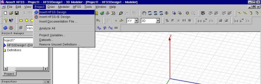
- Run Mosaic::Engineering::Electrical::HFSS
- MenuBar::Project::InsertHFSSdesign as illustrated below
- MenuBar::HFSS::SolutionType::DrivenModal
- MenuBar::Modeler::Units select mm
- Next draw the waveguide as a box: MenuBar::Draw::Box
And at the bottom of the screen enter x=0 y=0 z=0 mm,
and then type "enter "or "carriage return" then type
dx=100 dy=22.9 dz=10.2 mm, and then type "enter "or
"carriage return"
- Alterntively, click the DrawBox tool icon (yellow arrow
below), draw any box, click the "createBox" item (red arrow
below), and edit the properties (blue arrow below) to set the
Position=(0,0,0) and dimensions dx=100 dy=22.9 dz=10.2 mm as
given above.
- Press the "fitAll" toolbar item (orange arrow below) to view
the object.
when done it should look like:
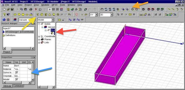
- Save a snapshot of the waveguide as above and paste it into
your report. ( P6 )
- MenuBar::View::FitAll::AllViews
- MenuBar::Edit::Select::Object then right-click the
waveguide and AssignMaterial air
MenuBar::Edit::Select::Faces then right-click the long
waveguide top face,
then right-click nextBehind to get the bottom plate, then
right-click assignBoundary Perfect-E
and repeat this for the long top face.
In the same fashion assign the two long sidewalls as
Perfect-E boundaries.
- Right-click the front face, and AssignExcitation::WavePort,
set name=input1,
next, numberofmodes=1, click on the integration line field and
select newline,
and draw a line from the center bottom of the port to the center
top of the new port,
click next, donot renormalize, and finish. Repeat this for
the output port.
- Highlight the excitation ports in the ProjectManger pane
(blue arrow below)
The ports and integration line should look like:
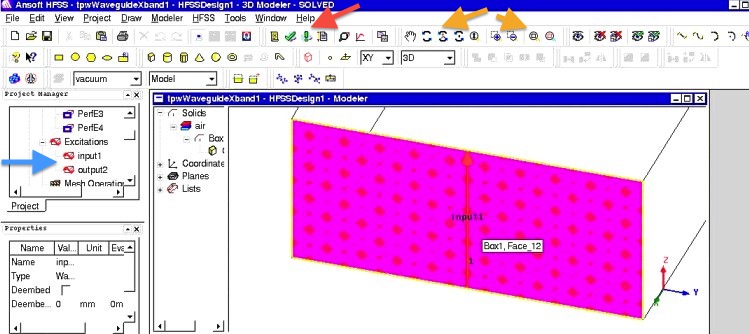
- The toolbar icons can be used to move the view (orange
arrows above)
- Save a snapshot of the one port as above and paste it into
your report. ( P7 )
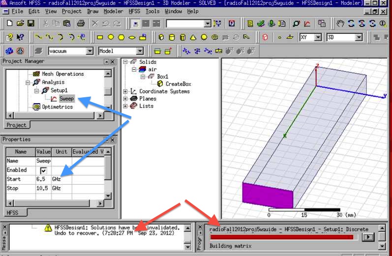
- MenuBar::HFSS::AnalysisSetup::AddSolutionSetup select
General::
SolutionFrequency 20 GHz, click OK
- MenuBar::HFSS::AnalysisSetup::AddFrequencySweep and linear
step sweep 6.0 to 16 GHz in 0.25 GHz steps, and
SweepType=discreet
- Your analysis and sweep should appear in the ProjectManager
pane (blue arrow below), where the sweep properties should
appear when the Sweep item is highlighted
- MenuBar::File::Save
- MenuBar::HFSS::ValidationCheck Everything should check
- MenuBar::HFSS::AnalyzeAll (red arrow above) to run the
simulation and watch for errors at the bottom message areas
(red arrows below)
- To see the results, run MenuBar::HFSS::Results::QuickReport
S-parameters
to plot the results (you may need to click a minimize icon to
show plots/reports hidden behind the top plot/report
Adjust you plot to go from -90 to 10 dBm and double click the
lines and make the width=3
and right-click and remove s12 and s22
Your plot should look like:
- Make sure that the legend does not obscure any portion of
your plotted curves (move it as above).
- Save a snapshot of the S-parameters as above, and paste it
into your report. ( P8
)
- Based on the dimensions
of the waveguide, what size waveguide is this (i.e.,
wr22,wr51,etc? (Q13) Hint http://en.wikipedia.org/wiki/Waveguide_(electromagnetism)
- What is the theoretical cutoff frequency of the lowest order
mode for the waveguide? (Q14)
Part 5
- Save a snapshot of the design as above and paste it into
your report. ( P9 )
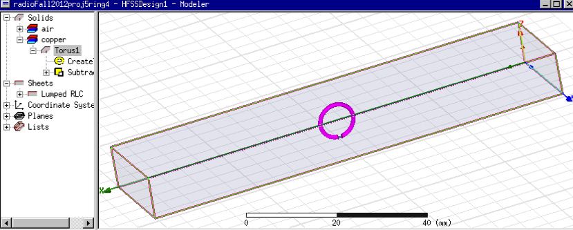
- Zoom in on the split ring (blue arrow below)
- Notice the lumped RLC sheet in the gap of the ring (red
arrow below). This behaves as a lumped component, a
capacitor, in the gap.
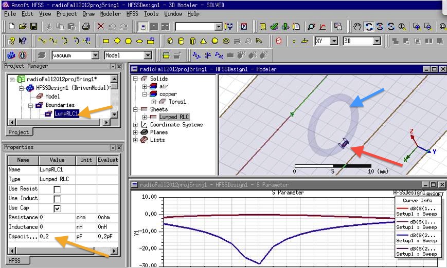
- Select the lumped RLC in the ProjectManager pane (yellow
arrow below) and observe the capacitance value (yellow
arrow below)
- Run the simulation
- When the simulation completes, select the first two results
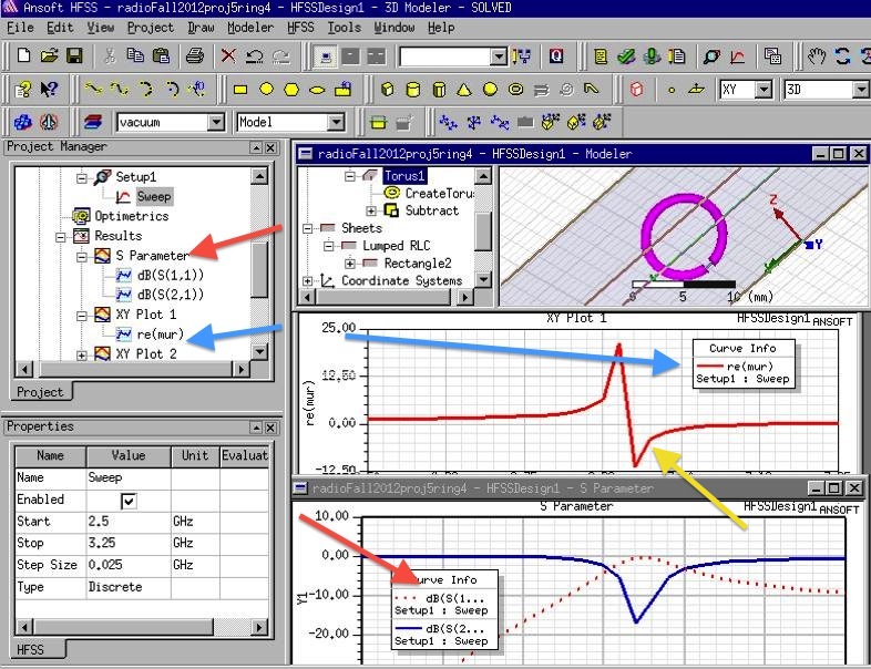
plots as illustrated below.
- Plot the relative
permeability as shown (blue arrows below) by
double-clicking XYplot1
- Plot the relativeS-parameters S11 and S21 as shown (red
arrows below) by double-clicking "Sparameter"
- Note the frequency range where the
relative permeability is negative (yellow arrow
above). This is the desied metamaterial behavior.
- Save a snapshot of the S-parameter plot as above, but with
all scales/axes visible, and paste it into your
report. ( P10 )
- Save a snapshot of the relative permeability plot as above,
but with all scales/axes visible, and paste it into your
report. ( P11 )
- From the capacitance value of the lumped RLC, and from the
frequency of the resonance in the S-parameters, compute the
inductance of the loop that resonates with the capacitance of
the lumped RLC. (Q15)
- Note, by right clicking results (in upper left pane of above
figure near red arrow) and selecting output variables, you can
see the formulas used to extract the mu and epsilon (generally
these are approximations below), See http://ieeexplore.ieee.org/xpls/abs_all.jsp?arnumber=1210783
for details on the formulas:
- dd = .01 (length in meters of the physical region
being characterized, typically the diameter of the ring)
- v1 = S(1,1)+S(2,1)
- v2 = S(2,1)-S(1,1)
- k0 = 6.28*Freq/3e8
- mur = 2/(cmplx(0,1)*k0*dd)*(1-v2)/(1+v2)
- epsr = mur+2*cmplx(0,1)/(k0*dd)
- epsr2 =
2/(cmplx(0,1)*k0*dd)*(1-v1)/(1+v1)
- Note: above formulas should be used when de-embedding is
up to within approx 1mm of edge of ring. To see
de-embedding, select Excitation in the upper left pane,
select the waveport, right-click properties, and click the
postprocessing tab. When the waveport is selected, you
should see an 3D arrow indicating how far the results are
deembedded from the waveport.
Part 6
- Use an excel spreadsheet (amp3.xls)
to calculate gain, Noise Figure, 1dB copmpression (P1dB), and
output intercept pount (OIP3) of the following system.
Paste the spreadsheet results into your report (P12 20 points)
Check some points by hand to prevent errors in using the
spreadsheet.
 .
.
Report
NOTE: Use the
Project
Report Template and
keep answers
to questions on consecutive sheets of paper with all plots at
the end.
Do not add extraneous pages or put
explanations on separate pages unless specifically directed to do
so. The instructor will not read extraneous pages!
Only turn in requested plots ( Pxx ) and requested answers to
questions ( Qxx ). All plots must be
labeled P1, P2, etc. and all questions must be numbered Q1, Q2,
etc. YOU MUST ADD CAPTIONS AND FIGURE NUMBERS TO ALL
FIGURES!!