Radio Frequency Design Project 3
Agilent ADS and Cadence 6 Software Tutorials, continued
Overview
Remain in same project groups for the
semester.
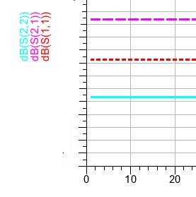
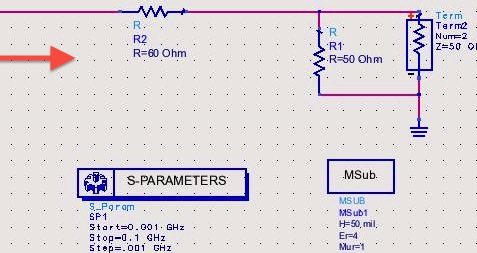
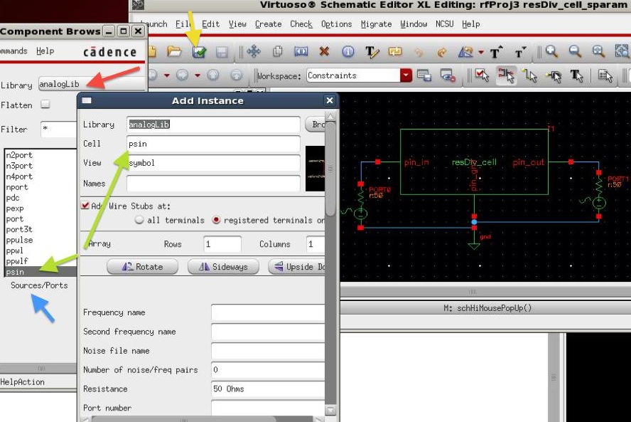
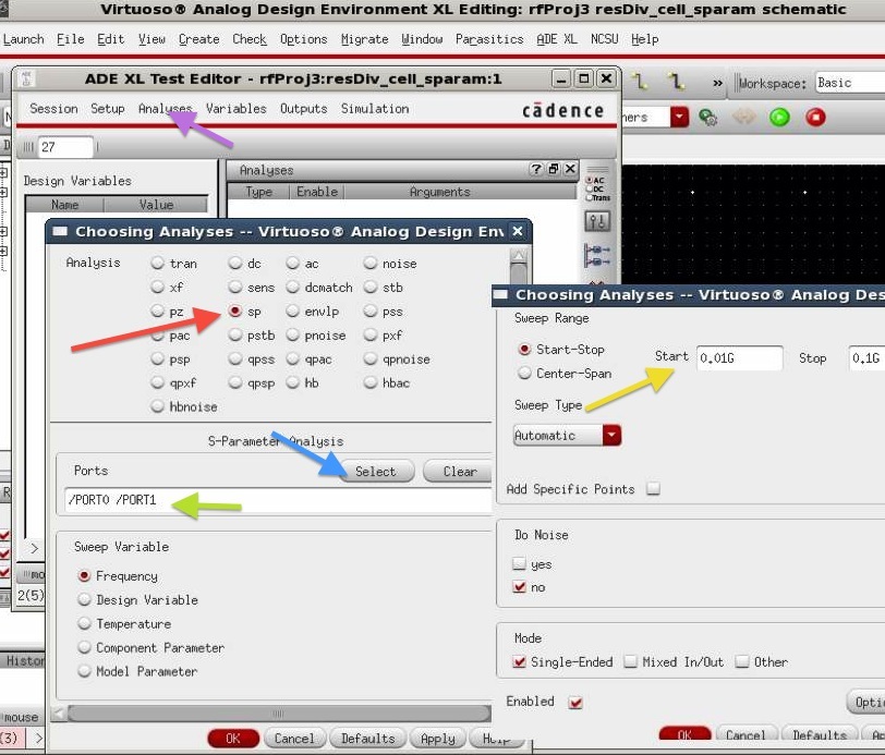
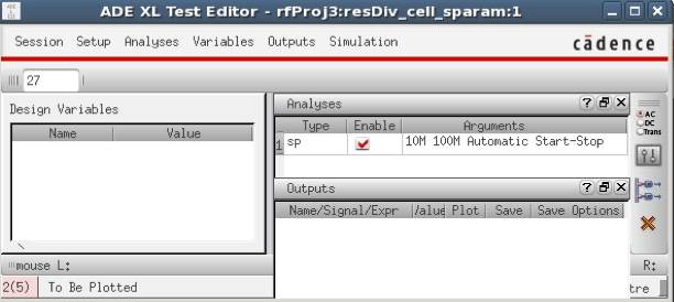
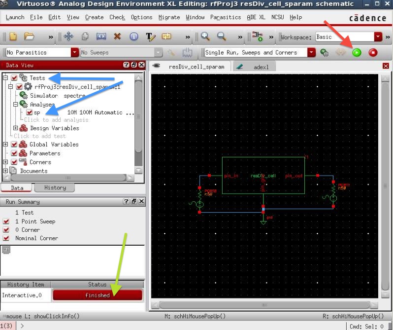
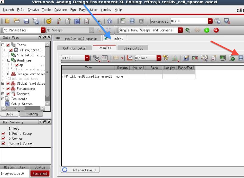
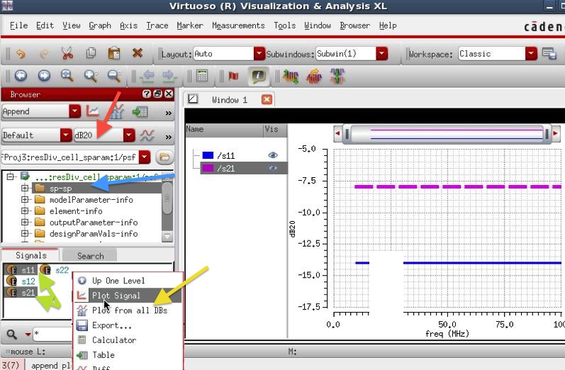
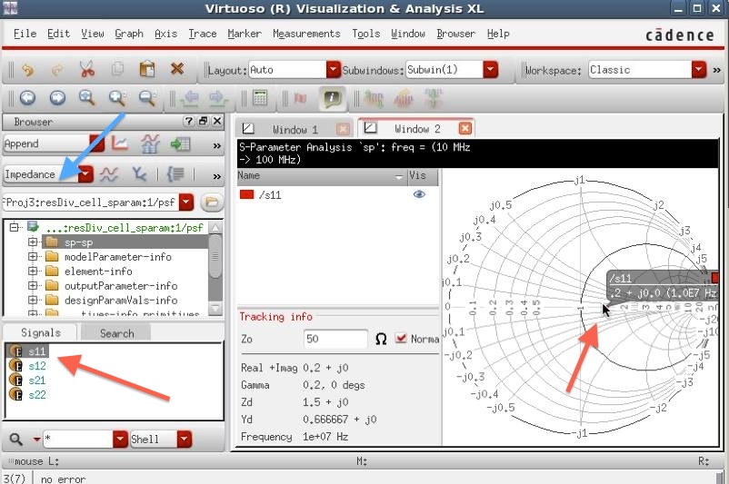
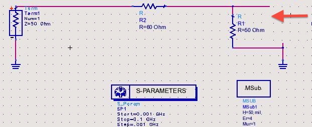
The objective of this project is to work with s-parameters
NOTE: Use the Project
Report Template and keep answers
to questions on consecutive sheets of paper with all plots at
the end.
IN NO CASE may code or files be exchanged between students, and
each student must answer the questions themselves and do their own
plots, NO COPYING of any sort! Nevertheless, students are
encouraged to collaborate in the lab session.
Only turn in requested plots ( Pxx )
and requested answers to questions ( Qxx ).
Part 1
Part 2
In this part, the behavior of a transmission line with
mismatch on one end is investigated.
Power conservation and issues of "where the power goes" are
explored.
Go down through the directory tree and open the schematic for
p2txline1, and double-click the p2txline1 schematic and
the following schematic should appear.
Save a snapshot of the schematic and paste it into your
report. ( P3 )
Double-click the "gear" icon (shown below) in the upper right
of the window to simulate.
Click the "rectangular plot" icon in the pop-up data plotting
tool.
Drop the plotting box in the visible area, and in the pop-up
window:
Select DataSet -> S(1,1) -> Add -> dB
Select DataSet -> S(2,1) -> Add -> dB
Select the plot options as shown below to plot S11 and S21 from -10 to 0 dB in 1 dB
steps. (the picture below may show -20 to zero)
Double-click each y-axis label to set the trace options for 2.5 point thick dot, short-dash, and solid
traces as shown below. You must do this so that the plots can be read when
printed in grayscale on a printer.
Save a snapshot of the s-parameters plot and paste it into
your report. You should have a "flat-line" plot of both
S11 and S21. ( P4 )
What is the line impedance? (from formula or linecalc).
Hint: check the MSUB item on the
schematic for substrate thickness and dielectric constant
( Q21 )
What is the total impedance to the
left of the line (i.e., what is the total source
impedance seen to the left of the line, the impedance of TERM1
)? ( Q22 )
What is the total impedance to the right of the line (i.e.,
what is the total load impedance seen to the right of the line,
as illustrated below)? ( Q23 )

And so ... you should conclude a mismatch with reflections.
Note that the S-parameters are plotted only from the
perspective of the TERM devices, so the power transmitted to the
right TERM device is only the power delivered to the TERM
resistor. (It doesnt "know" anything about what is going on with
the other resistor.)
Draw a schematic on a sheet of paper with a 50 ohm 2 volt rms
source (2Vrms open circuit) and a load comprised of two 50 ohm
resistors in parallel. At extremely
low frequencies, this is a good model of the circuit since
the transmission line is electrically short at dc (i.e.,
much less than a quarter wave). Questions Q24 - Q27
relate to hand calculations using this hand-drawn schematic.
What is the rms voltage across the two 50 ohm resistors
that are in parallel? ( Q24 )
What is the power in mW delivered to one of the two
parallel resistors.? ( Q25 )
What is the maximum power in mW available available from
the source (i.e., replace the two 50 ohm resistors with a
single 50 ohm load)? ( Q26 )
How many dB down is the power in Q5 relative to Q6? (10
log10( Q5/Q6 ) ) ( Q27 )
How does your answer to Q7 relate to the plot P4? ( Q28 )
... i.e., is there somewhere/something in the plot that
reflects this?
For Q29- Q33, assume that the maximum available power
from the source is 1 watt:
(The answers to the questions below
should agree with the foregoing calculations in Q4-Q8 AND
with plot P1 for the above ADS schematic at low frequency,
otherwise you have an error somewhere. The answers
should scale in proportion to the power sources.) )
What is power in mW delivered to the right-hand TERM
in the above ADS schematic? (This would correspond to
the power delivered to one of the two 50 ohm load
resistors in parallel in your hand-drawn schematic.) ( Q29 )
What is the power in mW delivered to the 50 ohm
resistor (not TERM) in the above ADS schematic? (This
would correspond to the power delivered to the second
one of the two 50 ohm loads in parallel in your
hand-drawn schematic.) ( Q30 )
What is the power in mW reflected back to the left
TERM in the above ADS schematic? (The left hand term
would correspond to the 50 ohm internal resistance of
the source in your hand-drawn schematic.) ( Q31 )
What is power delivered from the 1 watt source? (The
total power delivered to both load resistors in your
hand-drawn schematic.) ( Q32 )
Does the sum of the power delivered to the 50 ohm
resistor (not the TERMS) in the above ADS schematic plus
the power delivered to right-hand TERM plus the
reflected power equal the maximum available power? ( Q33 )
Click the "Smith plot" icon in the data plotting window,
shown below.

Drop the plotting box in the visible area, and in the pop-up
window:
Select DataSet -> S(1,1) -> Add
(only plot S11 on the Smith chart)
Click on the plot options, click Coordinate->both, select
Grid, and select admittance line type as long dash, and pick a
green color. Click OK and the Smith Chart should appear. To
figure out which end of the curve is at what frequency, Select
Marker->New from the Dataplot menu bar and click on one end
of the plotted curve. Then Edit->Undo to delete the marker.
(see below for an example of how the Smith chart should look
... depending on the shade of green you choose)
- Change the stop frequency of the simulation to 25
MHz, re-simulate the circuit, and Print the Smith
chart plot and turn it in. Note: You should have almost a
"circle"for the plotted data. ( P5 )
Part 3
In this part, simulations are performed on a simple
2-resistor voltage divider circuit using Cadence software.
From a Linux terminal, Cadence6/Virtuoso should be available
in the menu
(Mosaic->Engineering->Electrical->Cdence->Cadence6)
From a PC terminal, you must first open a remote Linux
session,
(Start->AllPrograms->Mosaic->LinuxConnect->ToAnyServer),
then proceed as for a Linux terminal
Create a new library "rfProj3" using
MenuBar::File::New::Library from the Library Manager menu bar,
and use the input parameters as shown below to create a 0.5
micron design
Make sure that you attach the proper tech library (ami 0.6u
c5n) as shown below
Note: sometimes the software hides the
popup window behind the windows
As shown below, highlight your new library on the left pane of
library manager window, and create a new cell named
"resDive_cell" using the MenuBar::File::New::CellView from
library manager menu bar.
This circuit will be a simple 2-resistor voltage divider
Always name your circuit cells
with the suffix "_cell" to indicate they are some smaller
subcircuit of a larger circuit
Make sure that the "open with"
option is "Schematics XL" (red arrow below)
NOTE: a common bug in Cadence is that
the "new file" popup window is hidden behind your other
windows
Next, add a pair of 50 ohm resistors from our
ami05_c6_customlib library to the schematic using the "create
instance" toolbar button at the red arrow below
Make sure you select the ami05_c6_customlib library (blue
arrow below)
Make sure you select the R50 device (green arrows below)
You can rearrange locations of things on your schematic by
using the "default selection" toolbar item (red arrow below)

Add the pins pin_in, pin_out, and pin_gnd using the "create
pin" toolbar buton at the red arrow below
Make sure all pins are inputOutput
as shown below (green arrows)
Wire the circuit using the wiring toolbar item shown at the
blue arrow below, and the final circuit should appear as follows
Check and save your schematic
using the "check and save" toolbar item at the yellow arrow
above.
If any errors are found, a popup should appear.
Print the schematic of your "resDiv_cell" as above and turn it
in. ( P6 )
Select one of your resistors, and type "q" on your keyboard,
and you should see the object properties popup as below, where
you can inspect/edit properties of a device
Next, create a symbol for your circuit using
MenuBar::Create::Cellview::FromCellview as illustrated below
In the popup shown below, make sure the toviewname is symbol,
fromviewname is schematic, and the type is schematicSymbol
In the pop-up, set the pin locations as follows (red arrows
below)
The symbol should be created as shown below (green arrow
below)
Check and save the symbol (red arrow above)
Close all of your schematic and symbol windows
Ceate a new schematic, as before.
Name this schematic "resDiv_cell_sparam"
Note: always name testbenches with a
prefix the same as the name of the cell being tested and with
a suffix indicating the test being done
This new circuit/cell will be the testbench (containing the
external test circuits) for doing s-parameter testing of the
"resDiv_cell" cell. Create the new testbench using
the MenuBar::File::New::CellView from library manager menu bar,
as shown below.
Make sure that the "open with" option is "Schematics XL"
Next, add an instance of our new "resDiv_cell" from our
rfProj3 library to the schematic by using the "create instance"
toolbar button at the red arrow below
Make sure you select the rfProj3 library (blue arrow below)
Make sure you select the resDiv_cell device (green arrows
below)
You should see your symbol appear in the schematic as shown
above, after you click in the schematic
(Sometimes if your cell has a odd center defined, the symbol
may be placed off-screen out of sight)
Next, add an instance of a ground symbol to your schematic by
using the create-instance toolbar button again The ground
comes from the analogLib sources/global library, as shown below
Next, add an instance of a "psin" port to your schematic using
the create-instance toolbar button again.
The psin port comes from the analogLib sources/ports library,
as shown below
Wire the schematic as shown above.
Check and save your schematic
using the "check and save" toolbar button at the yellow arrow
above.
If any errors are found, a pop-up should appear.
Save the schematic of your cell as above and turn it in.
( P7 )
Finally, create the simulation setup
Run ADE-XL from the MenuBar::Launch::ADEXL command in the
schematic editor of the new testbench as shown below
Make sure to use the "create new view" option on the popup
(blue arrow below)
The ADE-XL window should then appear as shown below
Click on the schematic tab (blue arrow above)
The testbed schematic should become visible as below
Then select MenuBar::ADEXL::Create::Test, as below:
The Test Edior window should appear (red arrow below), along
with the testbench being chosen:
Choose the cell of your testbench (blue arrow above), as in
the popup above, and click OK
The ADE-XL test editor should appear, as shown at the red
arrow above, behind the popup.
Note for future reference: If we used a variable in our
testbench, we would next need to run
MenuBar::Variables::CopyFromCellView to load them into the
window, and enter values for them in the window. We do not
have to do that here, since we have no variables defined in our
testbench schematic.
Click on the MenuBar::Analysis::Choose (purple arrow
below)
Set up the s-parameter analysis as follows:
Click the "sp" button for s-parameter analysis (red arrow
below)
Then, click the select button (blue arrow below) to enable you
to select your two "psin" sources from the schematic
After selecting, you should see ports "/PORT0 /PORT1" (green
arrow below).
Note for future reference: if this was a transient analysis
instead of s-parameters, you would select the output ports
using the MenuBar::Ouptputs::ToBePlotted::SelectOnSchematic
Note: a bit of an oddity is
that when plotting s-parameers S11 is for /PORT0 and S22 is for
/PORT1
Finally, set your sweep from 0.01 GHz to 0.1 GHZ (yellow arrow
below)
After clicking OK, the test editor should appear as below
Note that your new "sp" analysis should now appear in the
analyses pane
Return to your ADE-XL window, and in the left pane, expand the
"Tests" item to verify that the "sp" s-parameter analysis is
present (blue arrows below)
Then, click the green "run simulation" toolbar button (red
arrow below)
If the simulation runs properly, you should see "finished" in
the lower left corner area (green arrow below)
Return to the ADE-XL tab as below (blue arrow below)
Then, click the ResultsBrowser button (red arrow below) to see
the plotting window for s-parameters.
The Visualization and Analysis XL tool should appear as below
Select the "dB20" processing (red arrow below)
Select the "sp-sp" data (red arrow below)
Select S11 and S21 (green arrows below)
Right click over S11 and select the "Plot Signal" option
(yellow arrow below)
When the plot appears, the background will be black.
Right-click to set a white background as below.
Right-click the traces to set the
colors different as above, and with S11 as a solid line
"thick," and S21 as a dashed line "thick."
You should see the S-parameters plotted as above.
Save the plot of your s-parameters similar to above and turn
it in. ( P8 )
Hint: it is easy to check if your answers are correct by using
ADS to run the same simulation.
Change the "Default" near the red arrow above to "impedance"
as shown below (blue arrow below)
As before, right-click S11 (red arrow below) and choose
the "new window" plot option in the popup menu
Right-click::View::FitSmith in the Smith chart plotting area
to fit it as below
Save the plot of your Smith chart as above and turn it
in. ( P9 )
Finally, make sure to save all of your
test settings from within ADE-XL.
Use MenuBar::Session::SaveState from within TestEditor as
shown below
Make sure to save the state in the
CellView (red arrow below)
Note: If you closed Test Editor and the window is not open,
you can reopen it by right-clicking the test item under "Tests"
in "Data view" pane on the left side of the ADEXL window
Note: from within ADEXL there is a second type of saving an
overall ADEXL state from the ADEXL MenuBar as
MenuBar::File::SaveSetupState It does not appear that this
second type of saved state saves the test setup of the
test editor pane
You should be able to see your saved test state from within
Library Manager as follows, with the saved test setup
"spectre_state1" at the red arrow below
Save the image of your Library Manager showing your saved test
setup as above and turn it in. ( P10
)
We will talk more about the Smith chart next time
In the IEEE Microwave Symposium Jul 1991 paper "Recollections
on
microwave theory ," N. Marcuvitz describes in 1941
at MIT how they used their hands or cheeks to determine if
microwave energy was coming down a waveguide. This was before
high frequency detectors were widely available. (Note that
cellphones were in wide use 50 years later!) For even
greater sensitivity than the cheek, what part of their
face did they use to sense microwaves? (
Q34 )
In what year was the patent issued for the silicon catwhisker
crystal detector device (equivalent to silicon diode) to
Greenleaf Whittier Pickard (US Patent
836,531)? ( Q35 )
Report
NOTE: Use the
Project
Report Template and
keep answers
to questions on consecutive sheets of paper with all plots at
the end.
Do not add extraneous pages or put
explanations on separate pages unless specifically directed to do
so. The instructor will not read extraneous pages!
Only turn in requested plots ( Pxx ) and requested answers to
questions ( Qxx ). All plots must be
labeled P1, P2, etc. and all questions must be numbered Q1, Q2,
etc. YOU MUST ADD CAPTIONS AND FIGURE NUMBERS TO ALL
FIGURES!!
Copyright © 2010-2012 T. Weldon
Cadence, Spectre and Virtuoso are registered trademarks of
Cadence Design Systems, Inc., 2655 Seely Avenue, San Jose, CA
95134. Agilent and ADS are registered trademarks of Agilent
Technologies, Inc.