UNC Charlotte Agilent ADS and Cadence Software Tutorial
(Project 1)
Overview
First, form project groups for the
semester.
The objective of the tutorial is to become familiar with the basics
of Agilent ADS software and Cadence software.
NOTE: Use the Project
Report Template and keep answers
to questions on consecutive sheets of paper with all plots at
the end.
IN NO CASE may code or files be exchanged between students, and
each student must answer the questions themselves and do their own
plots, NO COPYING of any sort! Nevertheless, students are
encouraged to collaborate in the lab session.
Only turn in requested plots (Pxx )
and requested answers to questions (Qxx ).
Part 1
Part 2
Part 3
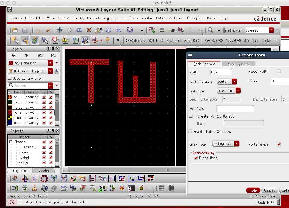
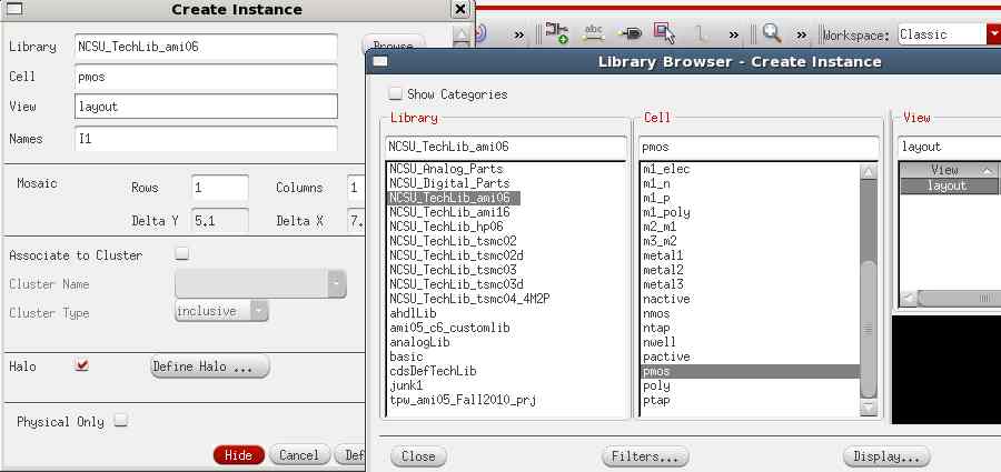
- Place the transistor near your initials as in the following
figure
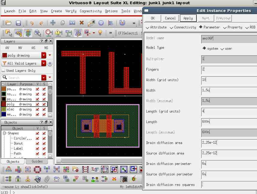
- Using MenuBar::Edit::Basic::Properties select the transistor
and edit the transistor property (2-finger gate) as follows:
Part 4
NOTE: Use
the Project Report Template
and keep answers to questions on
consecutive sheets of paper with all plots at the end.