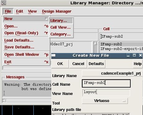
Cadence and Agilent ADS RFIC Design Tutorial
T.P. Weldon
Copyright 2010
Overview
This is a simple
tutorial for using Agilent ADS, Cadence, and our custom
libraries to design RFIC's. The libraries will greatly simplify
your effort.
In the following, you will be supplied with a Cadence library of IC
layout
components along with a companion schematic/simulation library for
Agilent ADS. Using these two libraries will save you many hours of
time. If you design a circuit using these library components, you
will be able to place all of your integrated circuit components in 5 minutes,
automatically. After component placement, you will only need to
wire the components
together.
Preliminary
tips and notes:
1. Download
and install the Agilent ADS library
Use
this Agilent ADS library for entering schematics for all circuits that
will be fabricated on your integrated circuits.
In your
schematics, only use the components included in the following library.
To minimize problems and confusion with prior projects,
you may want to move all old ADS projects and folders to a folder named
"old."
- Download the Agilent ADS Library
tpw_ami05_Fall2010_prj_ads.zip
- Extract this in your ADS directory
- Rename the tpw_ami05_Fall2010_prj directory with your initials
"xyz" replacing the
"tpw" above.
- You MUST rename it to
prevent problems when your chip is sent for fabrication
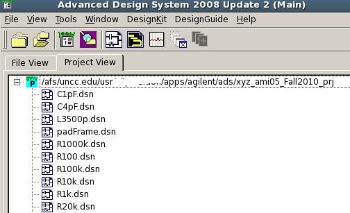
- Run ADS, and open the project, it should resemble the following
- You should construct your circuit design only using the
components included in the library, such as C1pf, R10k, R1k shown above.
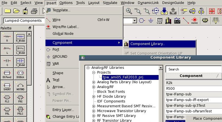
- To use these components in a schematic,
MenuBar::Insert::Component::ComponentLibrary as illustrated below
- Open the tpw-top-example schematic, it should contain the
following
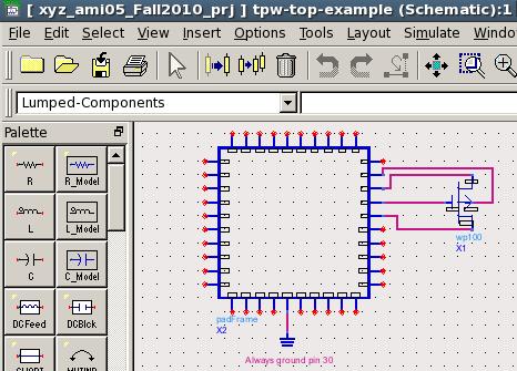
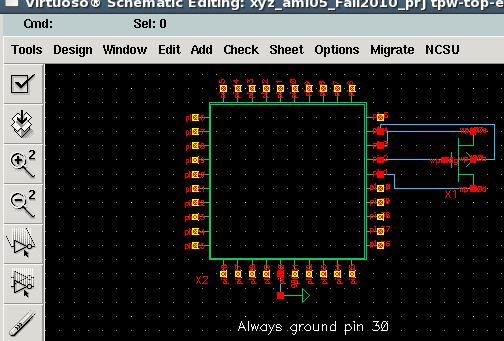
- The large 40-pin subcircuit is for the padframe, and you should
use this in your top-level schematic for layout of your integrated
circuit. It will result in automatic layout of your padframe
along with correctly numbered pins and ESD protection (static
protection on all pins).
- As a
rule, always ground pin 30 as shown in the example above.
Pin 30 has the shortest wirebonds.
- Connect your circuits to the padframe as shown above.
However, your final design should
not have transistors connecting to the padframe as shown above,
rather, you should have subcircuits connecting to the padframe.
- Descend through the padframe hierarchy to see the ESD
protection transistors. Select the padframe and push the button

- Return to the schematic and note that the transistor in the
schematic is actually one of the components from the library, wn50, a
50umx0.6um NMOS transistor.
- For an example of a subcircuit using the library components,
open the tpw-IFamp-sub schematic as shown below
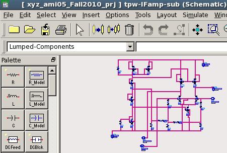
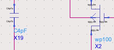
- If you zoom into the top left components, note that they a C4pF
capacitor and wp100 pmos FET. Both are from the component library
as shown below. Since they are subcircuits, they are numbered X19
and X2. You can descend into the subcircuit and see the circuit
and device parameters, just as any other subcircuit. Be careful not to
change any parameters of devices in the library!
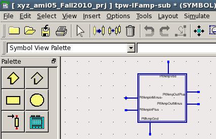
- View the tpw-IFamp-sub subcircuit symbol using
MenuBar::View::CreateEditASchematicSymbol and observe the symbol below.
- Use MenuBar::View::CreateEditASchematicSymbol to return to the
schematic
- Use
similar
naming conventions with your initials for your circuits, so the
instructor will be able to navigate through the final project that you
submit. This also helps prevent problems when all of the
integrated
circuits for our course are submitted for fabrication.
- To properly test your subcircuits, create a separate schematic
with the subcircuit symbol connected to the test equipmet as
illustrated in the transient test circuit tpw-IFamp-sub-transTest
transient test circuit illustrated below:
- Press the simulation button
 to
observe the transient output below:
to
observe the transient output below:
- Use MenuBar::Simulate::AnnotateDCsolution to observe bias
levels as below
- Push into the subcircuit hierarchy
 and
annotate the dc solution of the subcircuit.
and
annotate the dc solution of the subcircuit.
- Note the s-parameter test circuit and the intermodulation test
circuit that are also provided.
- Use
similar naming conventions with your initials for your circuits, so the
instructor will be able to navigate through the final project that you
submit. This also helps prevent problems when all of the
integrated circuits for our course are submitted for fabrication.
2. Download
and install the Cadence library
Use
this Cadence library for entering layouts for all circuits that will be
fabricated on your integrated circuits. Each component in
the Cadence library corresponds to a component in the ADS library, and
will be automatically created without you needing to enter every
component layout by hand.
In your
layouts, only use the components included in the following library.
!!!
STRONGLY RECOMMENDED: !!!
To minimize problems and confusion with prior projects,
you may want to move all old Cadence projects, libraries, and folders
to a folder named "cadence/NCSU/old"
and open Cadence and run MenuBar::File::DeleteLibrary to remove the old
libraries from the LibraryManager list.
- Download the Cadence AMI06
Library tpw_ami05_Fall2010_prj_cadence.zip
- See above recommendation to remove all old libraries from
Cadence before you do anything!
- Extract this in your cadence/NCSU directory
- Do not rename the directory yet,
it must be renamed from within Cadence
- Add the following line to the end of your cadence/NCSU/cds.lib
file:
- DEFINE tpw_ami05_Fall2010_prj
/afs/uncc.edu/usr/WHATEVER/linux/cadence/NCSU/tpw_ami05_Fall2010_prj
- where WHATEVER is your home directory path
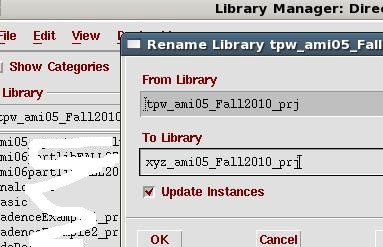
- Run Cadence
- From within Cadence, select the tpw_ami05_Fall2010_prj library
and then MenuBar:: Edit::Rename to rename the directory the same as
above with your initials "xyz" replacing the "tpw" (Cadence and ADS directory names MUST be
identical and end with _prj). Rename as below:
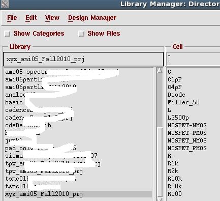
- Look in the new library. It should resemble the following:
- Open the schematic of example file tpw-top-example in
Cadence by clicking/highlighting on the
tpw-top-example in the cell column (as above), and double-clicking the
schematic in the view column (to the right of the cell column).
The schematic below should appear (corresponding to the ADS schematic
of the previous section).
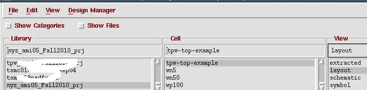
- Open the layout of the example file tpw-top-example in
Cadence by clicking/highlighting on the tpw-top-example in the
cell column (as above), and double-clicking the layout in the view
column (to the right of the cell column).
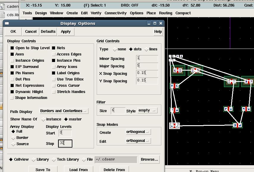
- Use MenuBar::Options::Display to see all layers and pins as
below:
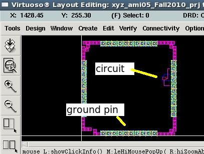
- The example chip should open as below ( )
- The ground pin is near the bottom center
- Do not forget to add a ground pin to your circuit and connect
it to the substrate using metal1 and ptap instanceas illistrated by
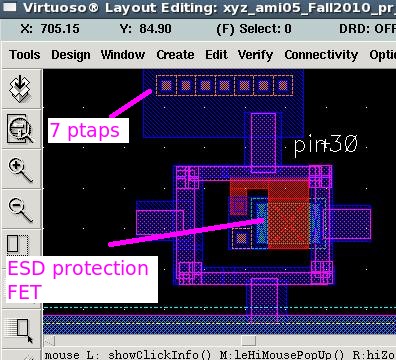
zooming in to pin 30 as shown below.
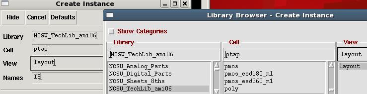
- For future reference, the ptap instances are created using
MenuBar::Create::Instance popup::library::Browse NCSU_TechLib_Ami06
cell ptap as illustrated below
- At the upper right of the layout, near pin 1, note the layout
of the transistor and its connection to the pins as illustrated below:
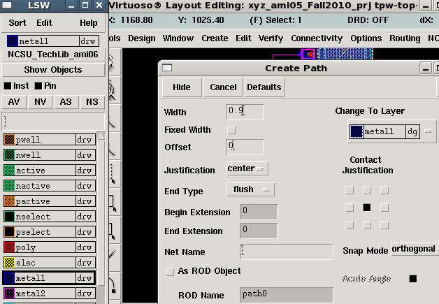
- For future reference, the wiring was done by first selecting
metal1 or metal2 in the LSW palette window, then using
MenuBat::Create::Path as below:
- Also, note that you can turn on "nets" to see where each
device should be connected to other devices based on the
schematic. To see these nets, use
MenuBar::Options::Display::Nets. (This example may not show nets,
due to the way it was created.)
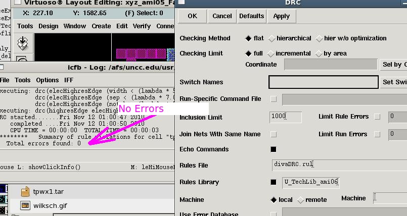
- Run DRC on the layout using MenuBar::Verify::DRC, and observe
that the icfb window shows no errors after it runs, as below
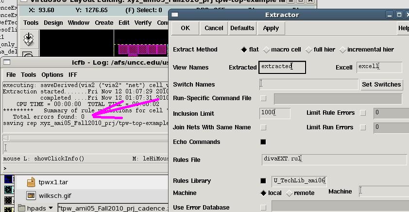
- Run extraction to prepare for LVS (layout versus schematic)
using MenuBar::Verify::Extract. as below.
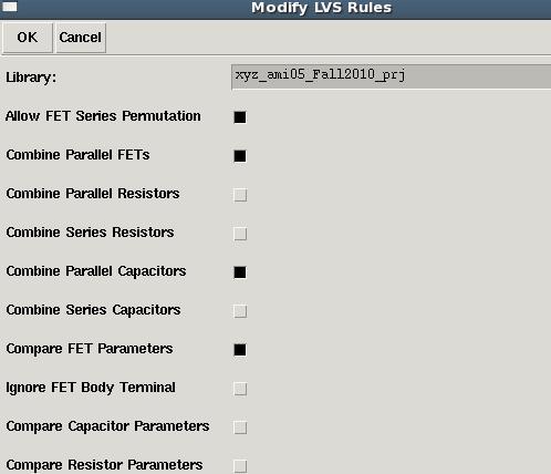
- Set the LVS options as below using the
MenuBar::NCSU::LVSoptions
- Make sure there are no errors as indicated in the icfb window
below (see arrow below)
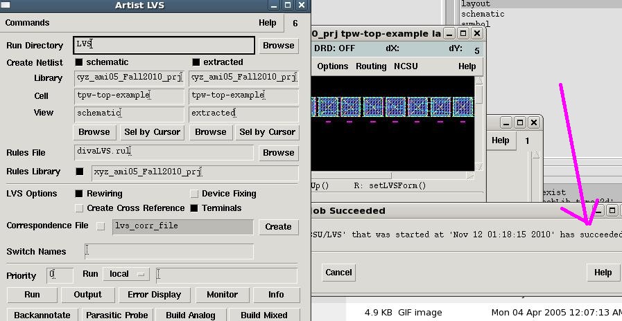
- Next run LVS (layout versus schematic) using
MenuBar::Verify::LVS as below. If a Forms Contents Different
window pops up, select "use form contents" and use the two browse
buttons below to select the schematic view and extracted views of the
tpw-top-example cell. After browsing, the form contents should be
as below. Then click on the RUN button, and look for the succeed
message popup below.
- WARNING:
succeed does NOT mean that your layout passed LVS, it only means
LVS ran completely without crashing.
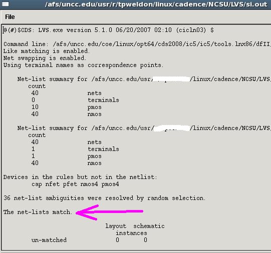
- Finally, you must check the LVS output to see if your layout
matches the schematic. Click the LVS button, and read the output
to check for errors or warnings. A successful LVS
MUST have the net-lists match message as below.
- IT IS
MANDATORY that all of your designs pass LVS at the top level including
the padframe. NO EXCEPTIONS!
- It would be good idea to create a zip-archive of your
Cadence project directory and your Agilent ADS project directory
- See Section 6 below if you get LVS errors
where
"netlists match logically but with mismatched parameters."
- As a
rule, consider saving backups of work frequently, so you can return to
a "known good" state.
- Other useful tips
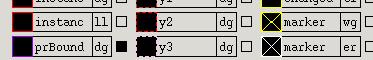
- To remove or resize a bounding box: First,
in the LSW window, LSW::Edit::SetValidLayers and add prBound dg by
checking the box as shown below
- After doing the above, you will be able to select the
box and delete it from the layout if desired
- If you have residual/remaining error/warning boxes use
MenuBar::Verify::Markers::DeleteAll, and run any necessary checks again
3. Example schematic and simulation using the library
The
schematic created in this section will later be exported for layout in
Cadence.
In your schematics, only use
components from the Agilent ADS library that was installed in Section 1
above.
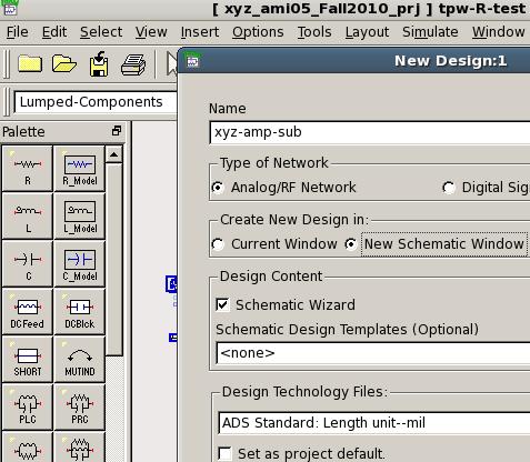
- Creating your ADS
Schematics
- Run Agilent ADS and
open your "xyz"_ami05_Fall2010_prj project
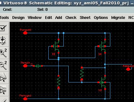
- Create a new schematic "xyz"-amp-sub using
MenuBar::File::NewDesign as below; (click "no help needed" in the popup)
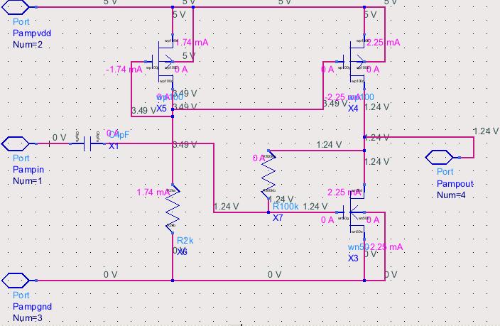
- Enter the following schematic (carefully note the devices from
the library, the names of the ports, and the absence of blue dots at
certain wire crossovers) The annotated voltages will appear
later, after simulation.
- There should be only one ground in the entire design, at the
top
level connected to pin 30 of the padframe. There should be no
ground
in any subcircuit, use a pin with a name such as "mysubcktgnd" in any
subcircuit.
- Do not connect all of your
circuits to a single vdd pin, since one
bad/oscillating circuit would then cause your whole chip to fail.
For
exmple, if your project was to create a negative indcutor and a
negative capacitor, have a separate vdd pin for each circuit so you
could disable one of them if it fails.
- Do not name any subcircuit pins "vdd" or "gnd",
since
these are
reserved system names/keywords. Instead, give your subcircuit
pins
names such as "abcAmpGnd" and "abcAmpVdd."
- All pins should be "InputOutput" type. Avoid using
"Input" or "Output" type pins.
- Do not
use pin names such as "vdd" or "gnd" to avoid problems with global
variable names
- To use these components in a schematic,
MenuBar::Insert::Component::ComponentLibrary and right-click the
component as illustrated below
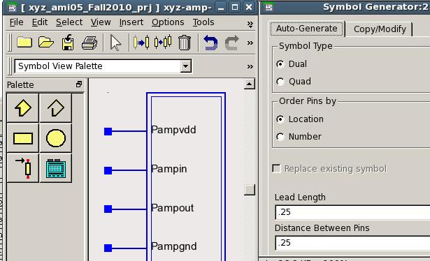
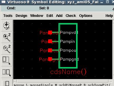
- Create a symbol for the schematic using
MenuBar::View::Create/EditSymbol as below. (If you wish, you can
rearrange pin locations from the defaults)
- Next, create a transient test circuit
"xyz"-amp-sub-transtest using MenuBar::File::NewDesign
- Place your new subcircuit in the schematic using
MenuBar::Insert::Component::ComponentLibrary and right-click the
component
- Place a ground pin using the
 button on the menu bar and wire it to Pampgnd pin (use the
  button to wire).
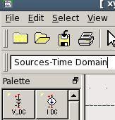
- Add a 5V dc source as below:
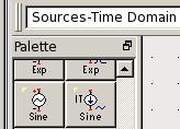
- Add an ac VtSine source at 10 MHz an 0.1 V as on the left
button below
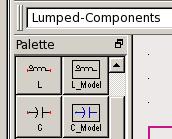
- Place a 2 nH in series with 5 pF load representing the output
loading of the IC package and PC board as below
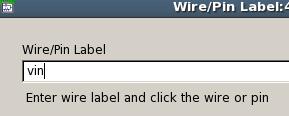
- Add wire labels vin and vout using MenuBar::Edit::WirePinLabel
as follows
- Add Simulation dc and transient simulation as below
- Finally, add the BSIM 3 models to your schematic by copying and
pasting them from the tpw-IFamp-sub-transTest schematic provided in the
ADS library. The final schematic should be as follows:
- Simulate the design using the simulate button
 and make sure the popup windows do not show errors.
- Use MenuBar::Simulate::AnnotateDCsolution to check that your
bias levels are correct. Push into the hierarchy of the symbol
using the button, and check the bias levels
in the subcircuit match the bias levels in the subcircuit schematic
given above.
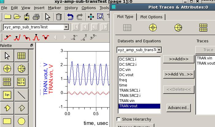
- Click the rectangular plot button in the popup, and add a plot
of vin and vout as follows:
- Fix any errors, so that your circuit is working properly.
- Save all of your work.
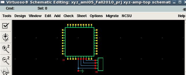
- Next, create another new schematic "xyz"-amp-top that will be
the top-level of your integrated circuit, including your padframe
- Only
use the word "top" in the name of only one schematic, to indicate the
top-level of your design!
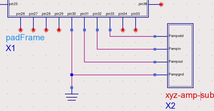
- Add the padframe compnent and your xyz-amp-sub as below.
Connect your amp to pins 31-34 of your padframe as below. Add a
ground to pin 30 as below. As shown below, share the ground pin
with ground and Pampgnd pin of your subcircuit, to save pins.
- It would be good idea to create a zip-archive of your
ADSproject directory
- As a
rule, consider saving backups of work frequently, so you can return to
a "known good" state.
4. Exporting
your ADS schematic to IFF format for layout
The
schematic created in Section 3 will be exported for layout in Cadence.
Make sure that your ADS project
directory "xyz"_ami05_Fall2010_prj and Cadence directoriy have the same
name before proceeding.
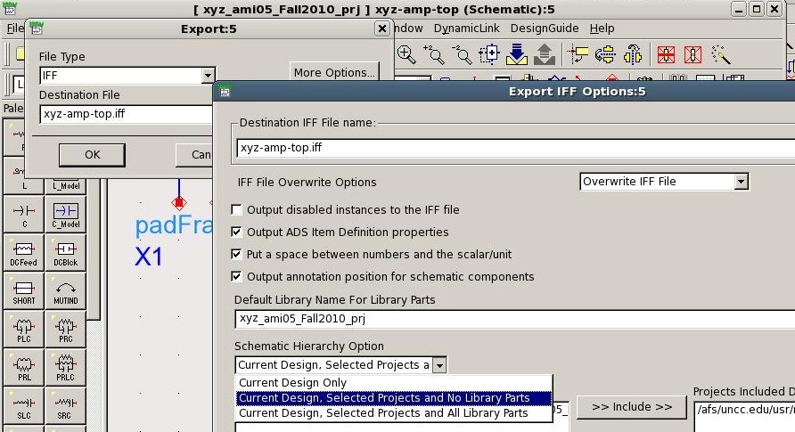
- Open your top-level schematic with the padframe, "xyz"-amp-top
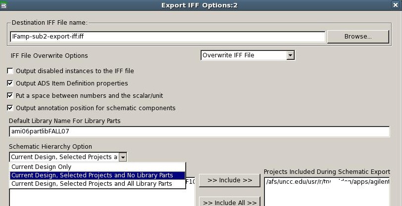
- Export an IFF file using MenuBar::File::Export with approriate
options set as illustrated below.
- The default library name should be the name of your project
directory, such as "xyz"_ami05_Fall2010_prj
- This will create a file in your ADS directory called
tpw-amp-top.iff.
5. Importing
your ADS schematic IFF file to Cadence for layout
The
IFF file created in Section 4 will be imported for layout in Cadence.
Make sure that
your ADS project directory "xyz"_ami05_Fall2010_prj and Cadence
directory have the same name before proceeding.
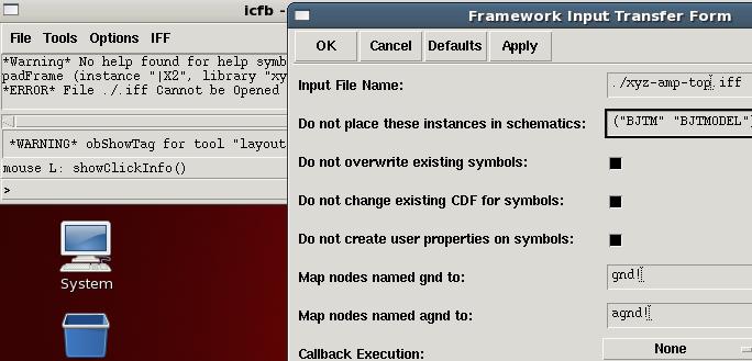
- Copy the IFF file tpw-amp-top.iff to your cadence/NCSU directory
- Run Cadence
- Make sure that you have
first installed and renamed the Cadence library
"xyz"_ami05_Fall2010_prj as described above in the installation
of the Cadence library
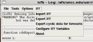
- To import the design: In the Cadence icfb window, run
MenuBar::IFF::ImportIFF as
below:
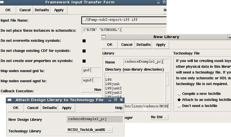
- If you are overwriting an
existing design, the safest way is to delete
it within Cadence before importing, since the "do not overwrite" option
is selected below.
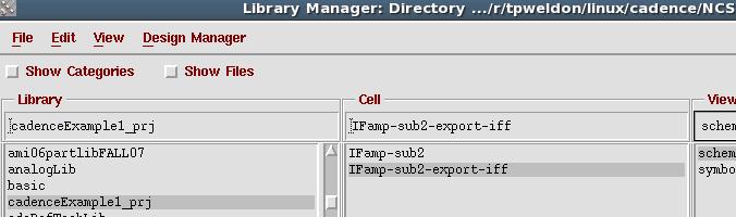
- Refresh the file view MenuBar::View::Refresh in the Cadence
Library manager window. Accept any "RefreshCDFs" popup.
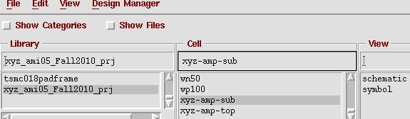
- You should now see your new schematics in the library:
xyz-amp-sub and xyz-amp-top as below
- Save all of your work
- Close Cadence
- It would be good idea to create a zip-archive of your
Cadence project directory and your Agilent ADS project directory
- As a
rule, consider saving backups of work frequently, so you can return to
a "known good" state.
- If you
accidentally corrupt the library, just re-extract the library and
overwrite your corrupted files. (You may have to rename the
library back to "tpw" before extraction)
6. Schematic-driven layout in Cadence
The
IFF file created in Section 4 will be imported for layout in Cadence.
Make sure that
your ADS project directory "xyz"_ami05_Fall2010_prj and Cadence
directory have the same name before proceeding.
- Run Cadence
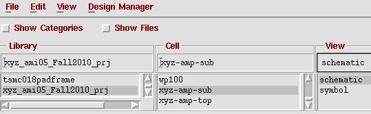
- In Library Manager, open the "xyz"-amp-sub schematic as below
- The schematic should be the same as your ADS schematic:
- In the Virtuoso schematic window, use
MenuBar::Check::CurrentCellView and observe the icfb window to
ensure there are no errors.
- From library manager, you can also open the symbol to check
that it is the same as in ADS:
- Next, return to the schematic in Virtuoso to begin
schematic-driven layout
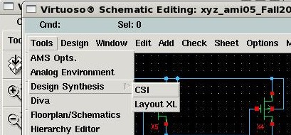
- From the schematic Menubar::Tools::DesignSynthesis::LayoutXL as
below. Click OK on the "create new" popup.
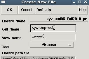
- And create new cell at the next popup as follows. Choose
the Tool=Virtuoso as shown below
- The Virtuoso layout window will appear
- Turn on Virtouso features with MenuBar::Tools::LayoutXL to
enable schematic-layout connectivity features
- Then from the Layout window use the command
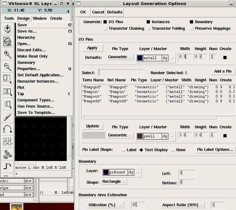
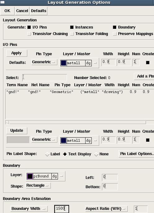
MenuBar::Design::GenFromSource as shown below.
- In the popup window below, make sure to:
- Set IO pins to metal1 geometric
- Click the APPLY button so all the pins listed in the box
switch from pwel to metal1
- Set pin label to text display (option height = 1 or 2)
- click OK
- Bounding box layer is not included in the normal palette, whic
makes them unadjustable. Tofix this issue,
in the LSW window use the menu bar command
LSWmenuBar::Edit::SetValidLayers and add "prBound dg" by
checking the box as shown below
- After doing the above, you will be able to select the
box and change/delete it from the layout if desired
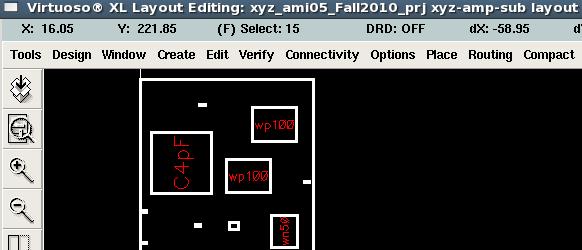
- Next, automatically place the devices in the Virtuoso layout
menu using MenuBar::Edit::PlaceAsInSchematic and the devices will
automatically be placed. Placement will not be perfect.
- Press the f-key on your keyboard to rescale the layout to fill
your screen
- Rearrange the devices roughly in the bounding box area as
below. (Select the whole area to see the tiny invisible parts)
- Shrink the bounding box at this point, if you wish
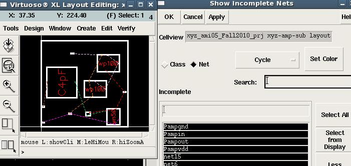
- Use MenuBar::Connectivity::ShowIncompleteNets and choose
SelectAll to see the connections that you must make, as below
- Note that when you select any device in the layout, the
corresponding device is highlighted in the schematic and vice-versa.
- You can hide the flight lines with
MenuBar::Connectivity::HideIncompleteNets
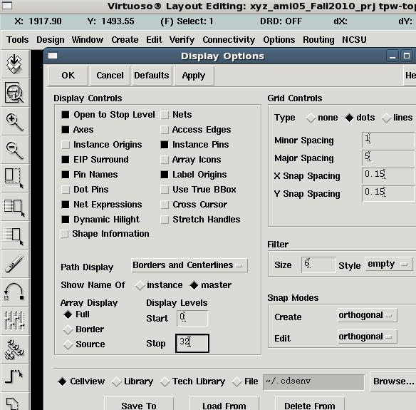
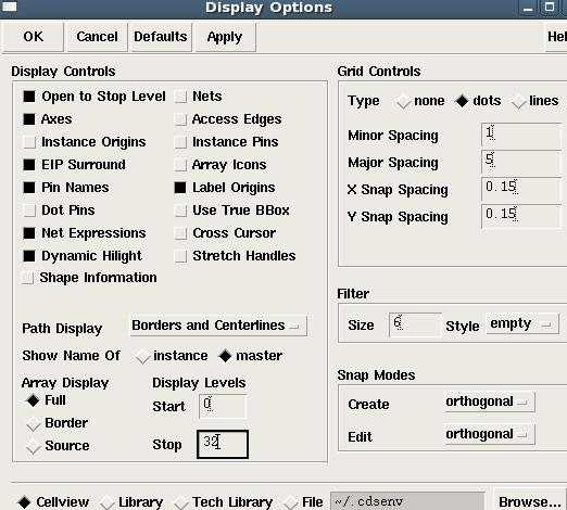
- Next, set MenuBar::Options::Display to check pinNames and
layers 1-32 as below
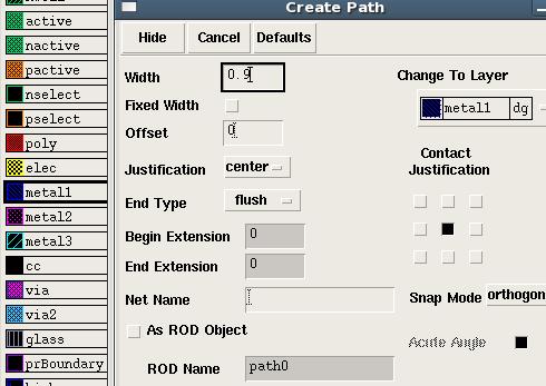
- Then choose metal1 or metal2 in the LSW palette and begin
connecting pins using MenuBar::Create::Path
- Run MenuBar::Verify::DRC frequently as you wire the circuit, to
catch errors as you work
- As you make connections the flight-lines should
disappear. (The layout editor is a bit particular, and will
require your path to cross over the pin before the flight line
disappears ... even when a connection is made to neighboring metal)
- Use MenuBar::Create::Contact to create vias between metal
layers (M2_M1) and contacts to the substrate (M1_P or ptap).
- Do NOT wait
until the end to do DRC!!
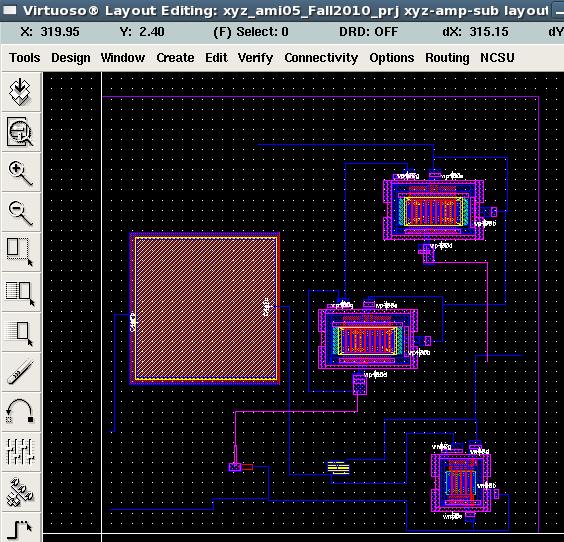
- Your final layout may look like:
- Final checks of your subcircuit
layout
- Run DRC with no errors: MenuBar::Verify::DRC (see DRC
examples above)
- Run Extraction with no errors: MenuBar::Verify::Extract
(see extraction examples above)
- Run LVS with no errors: MenuBar::Verify::LVS (see
LVS examples above)
- The
LVS output file must say "the netlists match"
- See below if you get LVS errors where
"netlists match logically but with mismatched parameters."
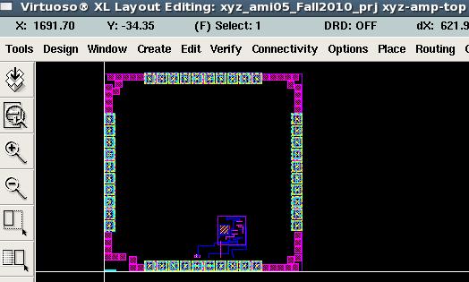
- Next, layout the top cell with the padframe,
- Open xyz-amp-top
schematic in Cadence Library Manager
- The schematic should be as follows:
- Run a check MenuBar::Check::CurrentCellView
- There are 34 warnings (yellow highlights above).
MenuBar::Check::FindMarker to see the warnings are for floating pins
- Next, return to the schematic in Virtuoso to begin
schematic-driven layout
- From the schematic Menubar::Tools::DesignSynthesis::LayoutXL
as below. Click OK on the "create new" popup.
- Next, begin schematic-driven layou as before for the subcircuitt
- From the schematic Menubar::Tools::DesignSynthesis::LayoutXL as
below. Click OK on the "create new" popup.
- As before, create new cell at the next popup as follows.
Choose the Tool=Virtuoso
- The Virtuoso layout window will appear
- Turn on Virtouso features with MenuBar::Tools::LayoutXL to
enable schematic-layout connectivity features
- Then from the Layout window use the command
MenuBar::Design::GenFromSource as shown below.
- In the popup window below, make sure to:
- Set IO pins to metal1 geometric
- Click the APPLY button so all the pins listed in the box
switch from pwel to metal1
- Set pin label to text display (option height = 1 or 2)
- set boundary width 1500
- click OK
- Bounding box layer is not included in the normal palette, whic
makes them unadjustable. Tofix this issue,
in the LSW window use the menu bar command
LSWmenuBar::Edit::SetValidLayers and add "prBound dg" by
checking the box as shown below
- After doing the above, you will be able to select the
box and change/delete it from the layout if desired
- Press the f-key on your keyboard to rescale the layout to fill
your screen
- Rearrange the devices roughly in the bounding box area. (Select
the whole area to see the tiny invisible parts)
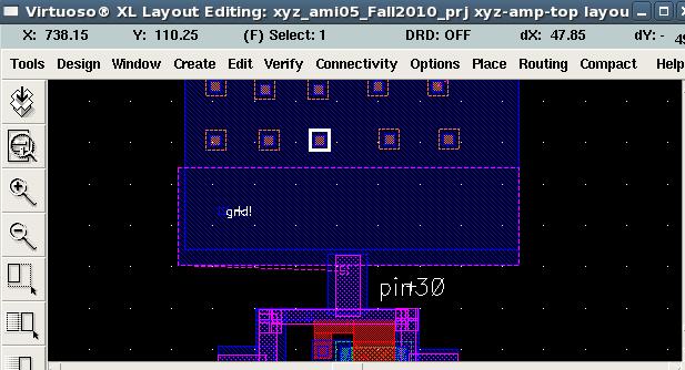
- Place the "gnd" pin near pin 30 and place the amp subcircuit
near pins 31-34 as below.
- Use MenuBar::Connectivity::ShowIncompleteNets and choose
SelectAll to see the connections that you must make, as below
- Note that when you select any device in the layout, the
corresponding device is highlighted in the schematic and vice-versa.
- You can hide the flight lines with
MenuBar::Connectivity::HideIncompleteNets
- Next, set MenuBar::Options::Display to check pinNames and
layers 1-32 as below
- Then choose metal1 or metal2 in the LSW palette and begin
connecting pins using MenuBar::Create::Path or
MenuBar::Create::Rectngle
- At the ground pin of pin 30, add 10 contacts to the substrate
below a large metal1 rectangle as shown below
- Connect all the remaining pins until your final layout is
completed as illustrated below:
- Final checks
of your integrated circuit layout
- Run DRC with no errors: MenuBar::Verify::DRC (see DRC
examples above)
- Run Extraction with no errors: MenuBar::Verify::Extract
(see extraction examples above)
- Run LVS with no errors: MenuBar::Verify::LVS (see
LVS examples above)
- The
LVS output file must say "the netlists match"
- If you get LVS errors where "netlists
match logically but with mismatched parameters," then you most
likely used incorrect settings when
you used the Cadence iff-import to import schematics, and you probably
accidentally
overwrote some Cadence library files. Typically, this type of error
will mention some 5 um
device was 0.6 um.
- To fix this LVS "mismatched parameter" error use
following steps
- make a backip zip of your cadence directory
before doing anything!
- then, download my original Cadence library,
and install it without changing the name to your initials.
- run cadence, and from within library manager,
copy my entire library into your library and overwrite everything. the
only things it will overwrite are the original library files that you
should not have changed anyway. If you get a pop-up window with
"fix-errors" and "overwrite" buttons at the bottom, first click
"fix-errors," then click "overwrite," then OK.
- Re-run LVS and the mismatch errors should not occur
- IT IS
MANDATORY that all of your designs pass LVS at the top level including
the padframe. NO EXCEPTIONS!
- It would be good idea to create a zip-archive of your
Cadence project directory and your Agilent ADS project directory
- As a
rule, consider saving backups of work frequently, so you can return to
a "known good" state.
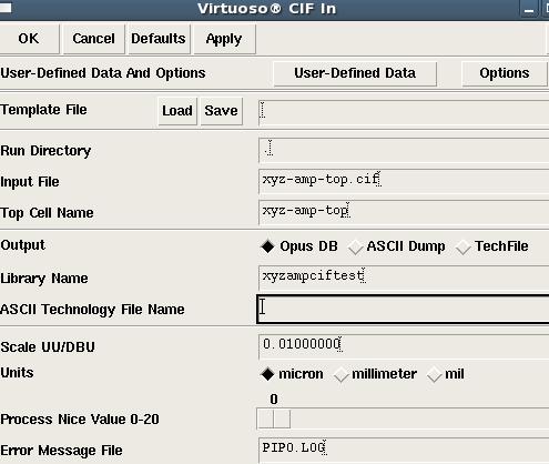
7. Exporting your design in cif format for MOSIS fabrication
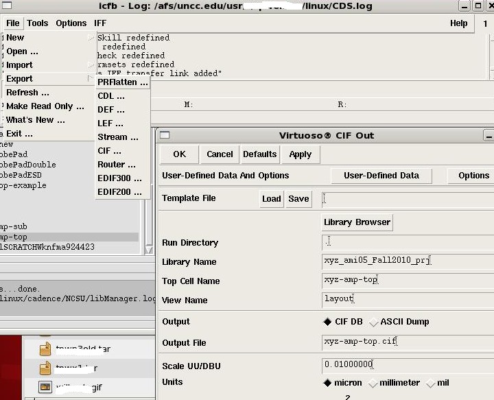
- Run Cadence
- From the icfb window MenuBar::File::Export::Cif as below
- Recheck the cif file by importing it and viewing it using icfb
MenuBar::File::Import:Cif as follows
- Edit the new library to attach the ami06 tech library using
MenuBar::Edit""AttachTechLibrary (because the full path to NCSU libs
above is a problem) Perhaps copying the techlib to your directory
would workaround this
- Note: there may be import errors/problems if the top layout cell has
the same name as the cif file. In this case, try renaming the cif file before
import.
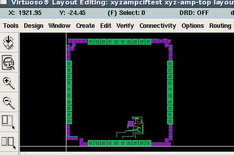
- The resulting layout should show the basic structure, even if
the layers are mislabeled as follows
- Another vendors cif-viewer would be a better check
- Finally, see the mosis website
for the latest submission details
8. Inductors
- Inductors do not seem to be supported well in the NCSU kit, so
some workarounds are necessary.
- A 3.5 nH inductor schematic and corresponding layout are provided.
- Only use the 3.5 nH inductor in your Agilent ADS library.
For accurate simulation, add a series resistor equal to the resistance
of the metal computed from the MOSIS ohms per square for each
metal. Metal3 and metal2 are in parallel.
- Export the inductor to Cadence in your schematic. It might
not lay out automatically in Cadence, since it has no pins/ports.
It was not possible to place pins on the inductor, because Cadence sees
the two pins as short-ciruited in the inductor.
- Two workarounds are needed:
- After export to cadence, and after placing the devices in
layout, delete the inductor from the Cadence schematic, replacing it
with a short circuit.
- Very carefully place and connect the inductor in the
layour.
- Take great care with this,
since LVS will not catch any errors with short-circuited inductors..
9. Other workarounds and tips
- If your help menus are not working, try directly accessing the
help tree through a browser
10. Other helpful websites
STOP HERE
STOP HERE
The following
methods are not required for our class,
they are used in full-custorm layout instead of using our library
components.
Exporting
ADS Schematics to Cadence
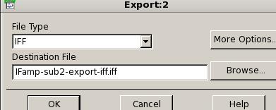
- Download the ADS file cadenceExample1_prj.zip in
N:/uncc/usr/r/tpweldon/pub/pubReadable (you must access this file
from a campus computer
- Extract the file in your ADS directory
- This ADS example shows you how to export an ADS schematic to
Cadence.
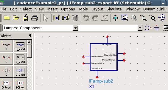
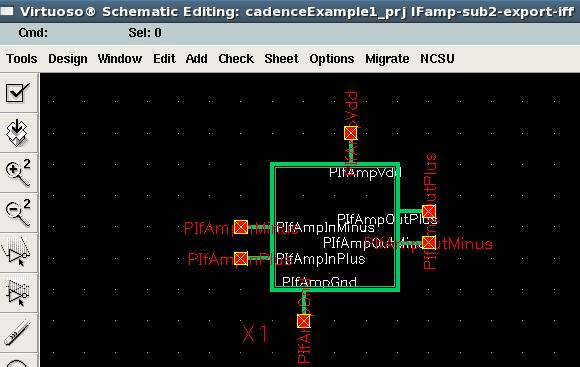
- Frst, make sure everything is installed properly by opening the
IFamp-sub2-transTest schematic, and run the transient test to see the
result below:
- For Full-Custom-Schematic-Driven-Layout (we will not do this)
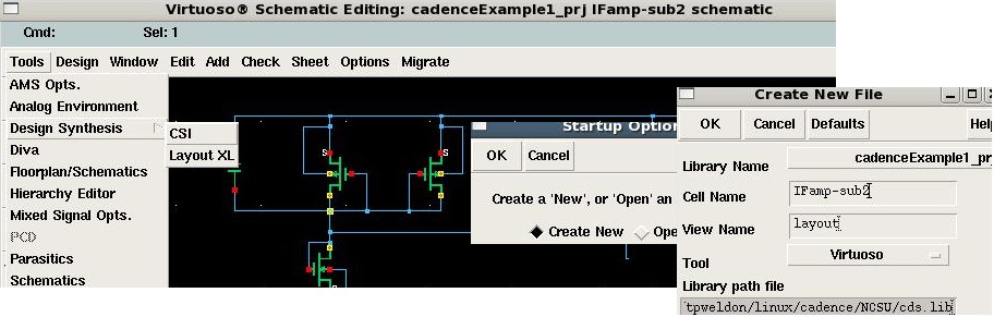
- From the schematic Menubar::Tools::DesignSynth::LayoutXL
- And create new cell
- And choose the Tool=Virtuoso as shown below
- To automatically create a Full-Custom-Schematic-Driven-Layout
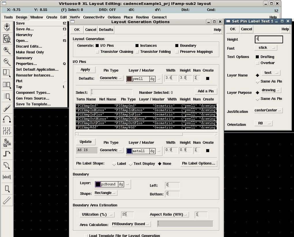
from the schematic, from the Layout window
MenuBar::Design::GenFromSource and select all the pins and metal1 and
click update so the pwells below change to metal1 as shown in the
options below
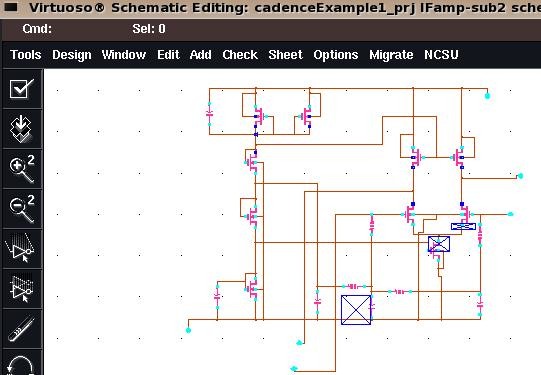
- The devices should be laid out approximately as in the
schematic as illustrated below.
- Set MenuBar::Display options to DisplayLevels:1-32, view nets
if desired , PinNamesif desired as below
- Note that when you click any device in the layout, the
corresponding device in the schematic is highlighted
- d
- ff
- To remove or resize a bounding box: First, in the LSW window,
LSW::Edit::SetValidLayers and add prBound dg by checking the box as
shown below
- Then you will be able to select the box and delete it from the
layout if desired
- If you have residual/remaining error/warning boxes use
MenuBar::Verify::Markers::DeleteAll, and run any necessary checks again