Microwave Circuits and
Metamaterials
Project 12
Overview
Remain in same project groups for the
semester.
The objective of this project is to investigate wideband
metamaterials.
NOTE: Use the Project Report Template and keep answers to questions on consecutive sheets
of paper with all plots at the end.
IN NO CASE may code or files be exchanged between students, and
each student must answer the questions themselves and do their own
plots, NO COPYING of any sort! Nevertheless, students are
encouraged to collaborate in the lab session.
Only turn in requested plots ( Pxx )
and requested answers to questions ( Qxx ).
Part 1
- In the following:
- You will investigate wideband metamaterials, and observe
negative relative
permeability and negative relative
permittivity
- The structure of the wideband negative
permittivity metamaterial consists of an I-beam with a negative capacitor in series with the
post, replacing the inductor that would normally tune the
center frequency of operation. The structure of the wideband negative permeability
metamaterial consists of an split ring with a negative inductor and negative capacitor
in the gap, replacing the capacitor that would normally tune
the center frequency of operation.
- The I-beam structure is closely related to capacitively
loaded strips (CLS as described in Design,
fabrication, and testing of double negative metamaterials
- The negative capacitors and negative inductors are examples
of circuit components that violate Foster's
reactance theorem
- Non-Foster circuits are often implemented using an NIC
(negative impedance converter) and/or implemented with current
conveyors that were introduced by Sedra and Smith around
1968
- Wideband non-Foster Negative Permittivity
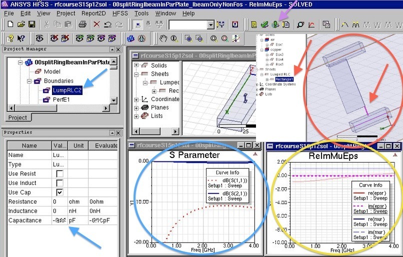
- Orient and zoom in on the Ibeam as shown in the red circle
above. Highlight the "Rectangle" RLC sheet (red arrows
above). Save a snapshot of the design as above and
paste it into your report. ( P1 )
- Make sure that your
plots, component
values,
legends, axes, and fonts are legible in your report!
- Determine the negative capacitance in the gap in the post of
the I-beam by selecting Boundary::LumpedRLC (blue arrows
above) that is placed in the gap (Rectangle at red
arrows above ). This "RLC" sheet is used as a
negative capacitor in the gap, to enable wideband negative permittivity using
the I-beam.
- What is the capacitance (blue arrows above) of the RLC sheet
in the gap of the post of the I-beam? (
Q3 )
- Run the simulation (purple
arrow above)
- Open the plot for S-parameters (blue circle above), and
paste a snapshot into your report. ( P2 )
- Open the plot for ReImMuEps (yellow circle above)
(real and imaginary parts of permittivity and permeability),
and paste a snapshot into your report. ( P3 )
- Non-zero imaginary parts of permittivity and permeability
indicate losses or gain in the material. Are the
imaginary parts of permittivity and permeability nearly zero
(lossless condition)? yes/no ( Q4
)
- What is the value of the real part of the permeability from 0.1 to 4 GHz, to
within +/- 0.1? ( Q5 )
- What is the value of the real part of the permittivity at 0.1 GHz? ( Q6 )
- What is the band of frequencies where the real part of the
permittivity is more negative than than -2.0, ... from 0.1 GHz
to ??? GHz? ( Q7 )
- What is the band of frequencies where the real part of the
permittivity is more negative than than -1.0, ... from 0.1 GHz
to ??? GHz? ( Q8 )
- Change the RLC sheet to -0.21 pF and rerun
the simulation.
- Replot ReImMuEps (yellow circle above) (real and
imaginary parts of permittivitty and permeability), and paste
a snapshot into your report. ( P4 )
- What is the new value of the real part of the permittivity
at 0.1 GHz? ( Q9 )
- This demonstrates that the non-Foster element has a profound effect on metamaterial
performance
- Wideband non-Foster Negative Permeability
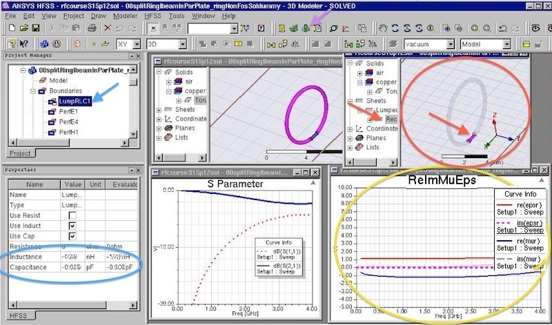
- Orient and zoom in on the split ring as shown in the red
circle above. Highlight the "Rectangle2" RLC sheet (red
arrows above). Save a snapshot of the design as above
and paste it into your report. ( P5 )
- Determine the negative capacitance and negative inductance
in the gap in split ring by selecting Boundary::LumpedRLC
(blue arrow above) that is placed in the gap (Rectangle
at red arrows above ). This "RLC" sheet is
used to enable wideband negative
permeability in the split ring.
- Note: to provide best wideband
performance, split rings should have both negative inductance
and negative capacitance in the gap. The negative
capacitance is necessary to compensate for inherent stray
capacitance in the gap (more details on this are given below).
- What is the capacitance and
inductance (blue circle above) of the RLC sheet in
the gap of the split ring? ( Q11 )
- Run the simulation (purple
arrow above)
- Open the plot for ReImMuEps (yellow circle above)
(real and imaginary parts of permittivity and permeability),
and paste a snapshot into your report. ( P6 )
- What is the value of the real part of the permeability at
0.1 GHz? ( Q12 )
- What is the band of frequencies where the real part of the
permeability is more negative than than -2.0, ... from ??? GHz
to ??? GHz? ( Q13 )
- This example again demonstrates that the non-Foster element
has a profound effect on
metamaterial performance
- Exit the program, File->Exit
NOTE ReportTemplate: Use the Project Report Template
and keep answers to questions on
consecutive sheets of paper with all plots at the end.
Do not add extraneous pages or put explanations on separate
pages unless specifically directed to do so. The instructor will
not read extraneous pages!
Only turn in requested plots (Pxx )
and requested answers to questions (Qxx ).
All plots must be labeled P1, P2, etc. and all questions must be
numbered Q1, Q2, etc. YOU MUST ADD CAPTIONS AND FIGURE
NUMBERS TO ALL FIGURES!!
Copyright 2010-2015 T. Weldon
Cadence, Spectre and Virtuoso are registered trademarks of
Cadence Design Systems, Inc., 2655 Seely Avenue, San Jose, CA
95134. Agilent and ADS are registered trademarks of Agilent
Technologies, Inc.