Microwave Circuits and
Metamaterials
Project 5
Overview
Remain in same project groups for the
semester.
The objective of this project is to layout a simple integrated
circuit using the Cadence software.
NOTE: Use the Project Report Template and keep answers to questions on consecutive sheets
of paper with all plots at the end.
IN NO CASE may code or files be exchanged between students, and
each student must answer the questions themselves and do their own
plots, NO COPYING of any sort! Nevertheless, students are
encouraged to collaborate in the lab session.
Only turn in requested plots (Pxx )
and requested answers to questions (Qxx ).
Part 1
- In this part, you will layout an integrated circuit using the
Cadence software..
- You will use the RF amplifier design from the previous
project
- For a list of rules see MOSIS.com
ON Semiconductor C5N SCMOS_SUBM
rules
- Load and run your project from the prior session:
- You will use the previous project
- Run ADS simulator and open the new workbook by
double-clicking it
- You should have a library named rfproj6 from the last
session
- Warning on
resistors in Cadence6
ami05_c6_customlib
- In post-2014 installations of the Cadence6
ami05_c6_customlib, the resistors (R50, R100, R1K, etc) may
not function properly in simulations. To correct this
problem, open the schematic of each resistor in the library
and replace the existing resistor in the resistor schematic
with a new resistor from the library NCSUAnalogParts::RLC::res
having the proper value. Then, check and save the
schematic, open the layous, extract the layout, and run LVS to
finalize the change. Then, check and save the resistor
cell schematic, open the layout, extract the layout, and run
LVS to finalize the change. Simulation should run correctly
after this. You may wish to check your repairs to
the library by simulating the dc voltages in a simple voltage
divider.
- Creating a top-level schematic with a padframe
- You will first create a very simple layout, including
padframe and ground pin
- Note: Pin 30 MUST ALWAYS BE GROUNDED
as described below
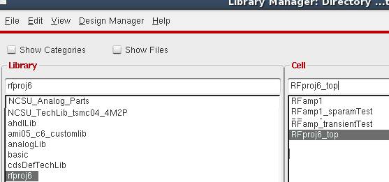
- In LibraryManager (below), in the rfproj6 directory, create
a new cell schematic (schematicXL) named rfproj6_top using
MenuBar::File::New::CellView
- This represents the "top" or highest level in your design
hierarchy
- Only use the word "top" in one cell
view in any future projects, so it can easily be found
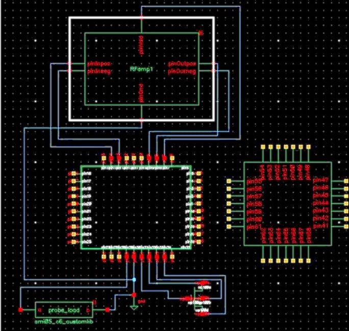
- Place the following instances (blue arrow below) on the
schematic
- a probe_load from Library
ami05_c6_customlib, Note: pin "b" must be
grounded on this device
- a padframe_2200 from from ami05_c6_customlib,
- a wp100 from from Library ami05_c6_customlib,
- and a "gnd" from Library analogLib/Sources/Globals
- NEVER NEVER NEVER use "gnd" pins
anywhere except in the top-level schematic
where the padframe exists. If at all possible, only use
one "gnd" pin in your entire design, no matter how many levels
deep the schematic hierarchy may be
- probe_load is a calibration circuit for s-parameter
measurement on chip, pin "b" must be grounded on this
device
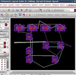
- Wire the schematic as shown below, check and save the design
( 62 warnings for unused pins)
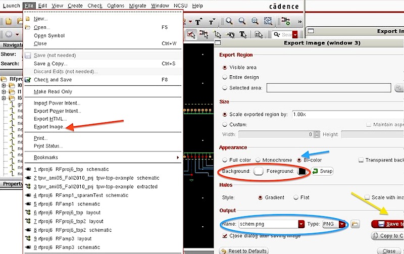
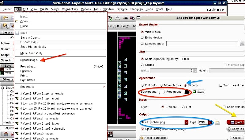
- Plot your schematic with a white background. To export
a schematic with white background, use
MenuBar::File::ExportImage (red arrow below) and change the
background to white and foreground black (red circle below),
if desired set bi-color (blue arrow below), enter the file
name (blue circle below) and save the file (yellow arrow
below) ( P1 )
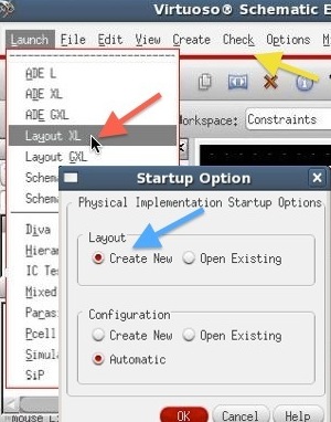
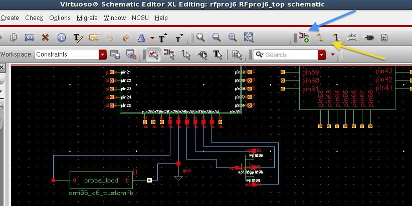
- Llaunch the Layout XL tool (red arrow below)
- In the popup window, select create new (blue arrow below)
- Schematic-Driven Layout
- Components from the library are automatically placed using
schematic-driven layout
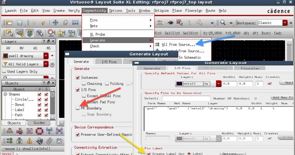
- In the Layout XL window, create a new layout using
MenuBar::Connectivity::Generate::AllFromSource (blue
arrow below)
- In the popup options windows, check the tabs for the
options and make sure PR boundary (place and route
boundary) is turned off as below (red arrow below)
- In the popup, click the IO pins tab and Make sure that the
create label option is turned on (yellow arrow below), and
metal1 or metal2 is shown as the layer
- Note that the "gnd!" pin from your schematic will be created
as metal1 0.9x0.9 micron pin
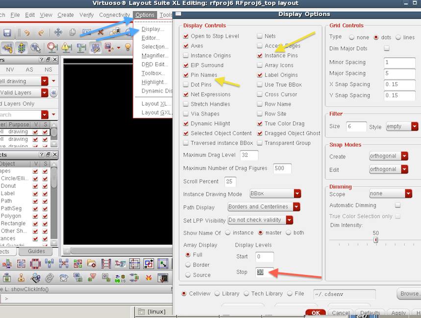
- As before in Layout XL, use MenuBar::Options::Display (blue
arrows below) to set the "Display Levels" to 0 to 30 (red
arrow below), and to set the check buttons "on" for "Pin
Names" and "Instance Pins."(yellow arrows below)
- Before doing anything else, select the padframe, type "q" on
the keyboard, and set the padframe at
coordinates 0,0 (blue arrows below)
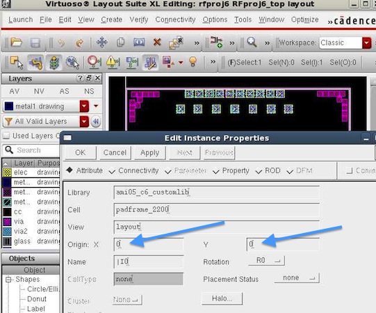
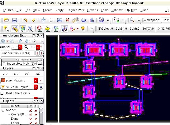
- Rearrange your layout as shown below
- Note: the very tiny "gnd!" pin will be hard to locate near
the 0,0 coordinate
- NEVER NEVER NEVER use "gnd" pins
anywhere except in the top-level schematic
- Place your probe_load and wp100 as shown below (yellow
arrows below)
- Selecting a pin or device in the layout highlights the
corresponding item in the schematic
- Activate the annotation browser pane using
MenuBar::Window::Assistants::AnnotationBrowser
- Then, use MenuBar::Connectivity::Nets::ShowAllIncompleteNets
to see the nets that must be connected
- You can move devices by typing "m" in the layout area
- Then, move your pins and devices into positions
approximately as below, where the nets will be easy to connect
and wire
- Set the ground pin "gnd" near pin 30 wirebond pad (bottom
center of padframe)... further details later
- In a fabricated layout, cell for
probe_load must be placed in an area where the probe will
not bump into wirebonds
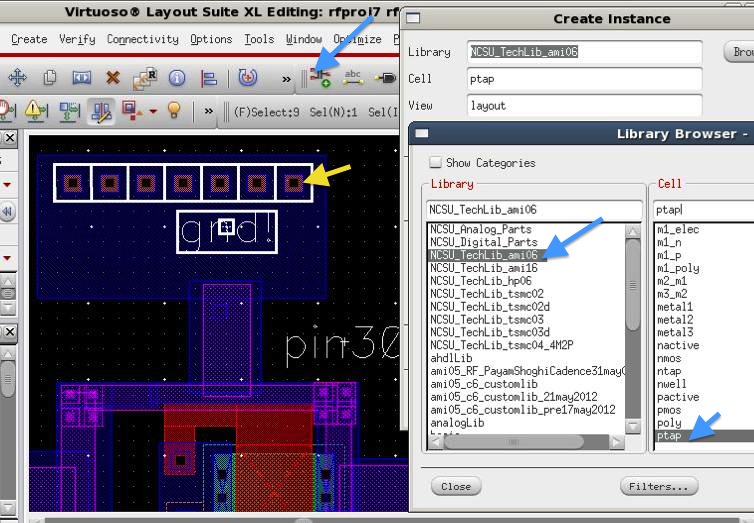
- Place your "gnd!" pin as below on pin 30
- Connect the gnd! pin to the substrate using metal1 (select
metal 1 in the palette and type "r" on the keyboard to draw a
metal1 rectangle)
- Then, add 7 "ptap" instances (yellow arrow below) in the
metal1 rectangle area as shown below, using the addInstance
button (blue arrows below)
- The ptaps connect the ground pin to the substrate, thereby
grounding the p-type substrate of the integrated circuit chip
- Always use pin 30 for ground, since it
has the shortest wirebonds with the lowest inductance
- The Pin 30 ground pin layout should appear as
illustrated below.
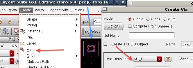
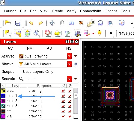
- As an alternative, you can create a ptap as an M1_p via
using MenuBar::Create::Via (lef t red arrow below) and
choosing M1_p (right red arrow below) to place the M1_p via
seen at the blue arrow below This is the same structure
as a ptap
- Plot your Pin 30 layout as above with a white
bacground. To export a layout with white background, use
MenuBar::File::ExportImage (red arrow below) and change the
background to white and foreground black (red circle below),
if desired set bi-color (blue arrow below), enter the file
name (blue circle below) and save the file (yellow arrow
below) ( P2)
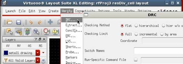
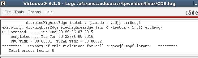
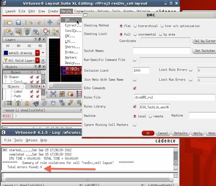
- Run DRC (Design Rule Check) as illustrated below
- Check the Cadence Command Interpreter Window (error log) to
see there were no DRC errors as shown below
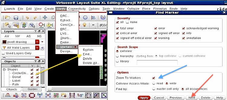
- If you have DRC errors,
immediately after running DRC check, use
MenuBar::Verify::Markers::Find (yellow arrow below)
- In the popup, select Zoom to zoom to the error (blue arrow
below)
- Click next (red arrow below) to proceed to the error in the
layout
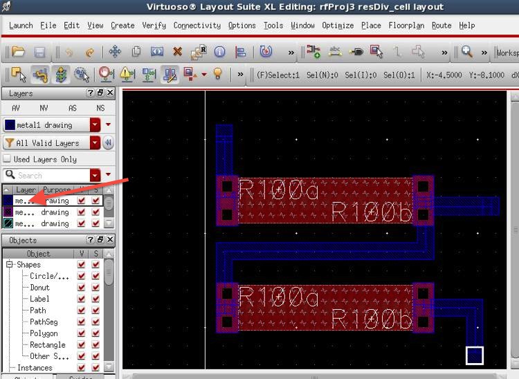
- Next, wire the transistor
- Select metal1 (blue arrow below) on the LayersPalette in the
left side of the Layout XL window, then type "p" on the
keyboard when your mouse is in the layout area to create a
metal1 path. (Alternatively use
MenuBar::Create::Shape::Path)
- Connect your wp100 circuit as illustrated below using metal1
and/or metal 2 paths
- Experiment with typing "r" in the layout area to draw a
metal1 or metal2 rectangle
- Note that the pins on the transistors
have both metal1 and metal2 contact areas so that you
have the option of using metal1 or metal2 to wire any
pin. the same is true for the padframe pins
- See notes later below, if you need to use a via to make a
connection from metal1 to metal2
- For a list of rules see MOSIS.com
ON Semiconductor C5N SCMOS_SUBM
rules
- Plot your wp100 layout as above (
P3 )
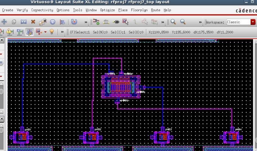
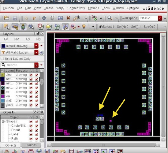
- Your final layout should appear as below:
- Plot your overall layout as above ( P4 )
- Finally, perform DRC, Extraction, and LVS (Layout Versus
Schematic) as described below
- Check the Cadence Command Interpreter Window (error log) to
see there were no DRC errors as shown below
- Save your layout
- It is a very good idea to do a
DRC check and save your file every 5 minutes!
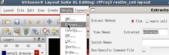
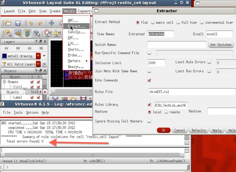
- Run Extraction as illustrated below
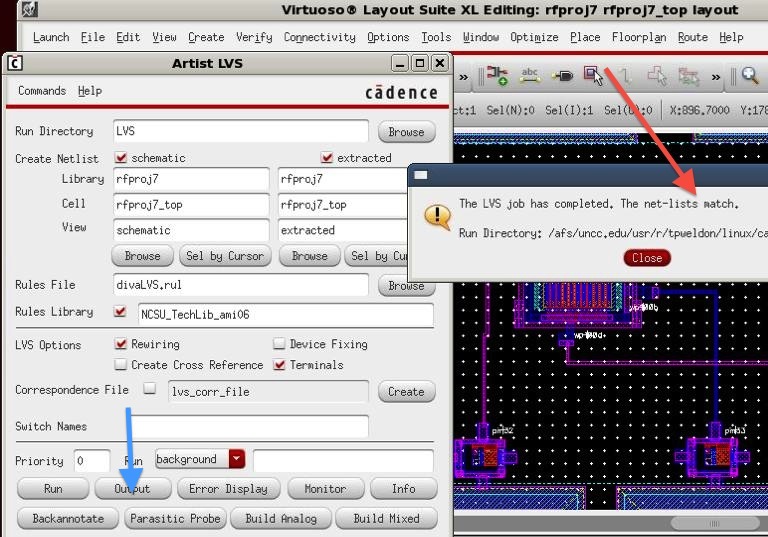
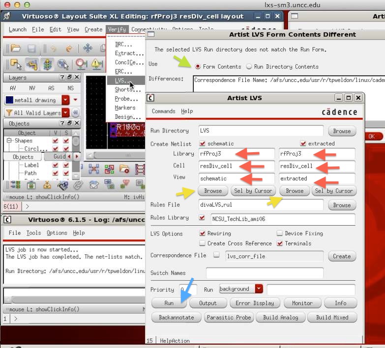
- Run LVS as illustrated below
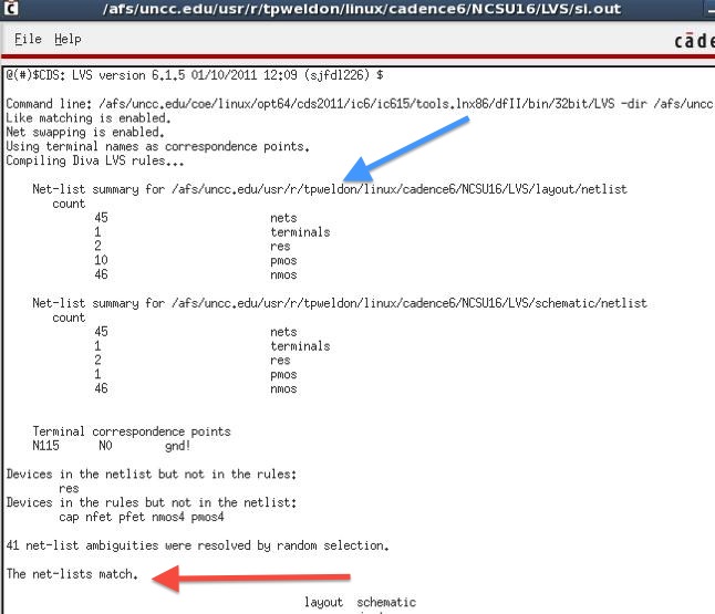
- The netlists must match! (red
arrow below)
- Inspect the LVS output by pressing the output button (blue
arrow above)
- The output should appear as below
- Print your LVS output as above and make sure to include your
home directory (blue arrow above) and netlists match (red
arrow above) ( P5 )
- Save your layout
- It is a very good idea to do a
DRC check and save your file every 5 minutes!
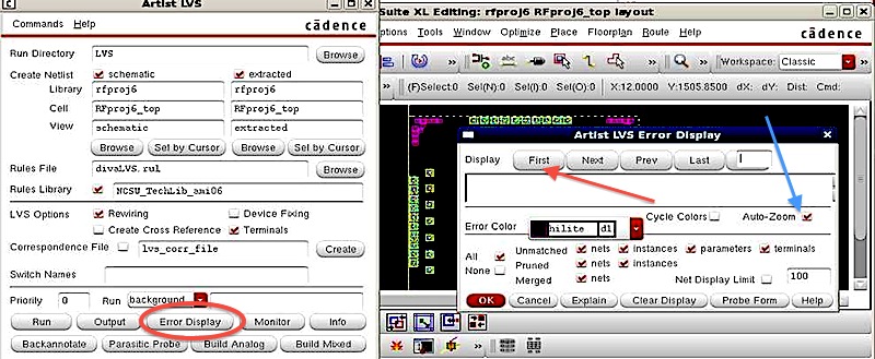
- If you have LVS errors,
immediately after running LVS, use click the ErrorDisplay
button (orange circle below)
- In the popup, select Zoom to zoom to the error (blue arrow
below)
- You must select either the schematic
view or extracted view before the next step
- Click First (red arrow below) to proceed to the error in the
schematic or extracted view
- Creating a symbol for your RF amp Cell
- Close all open layouts and schematics
- Please note that your project already
comes with a symbol view (blue arrow below) as shown
below
- If you wish to see details on
how you could create a symbol from scratch, see the
supplementary material at project05_s15supplementCreateSymbol.html
- Make sure that none of your pins have names that could
interfere with global names/variables.
- NEVER name a pin "gnd" or "vdd" or
"vcc" or "vss"
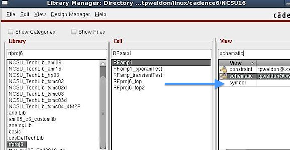
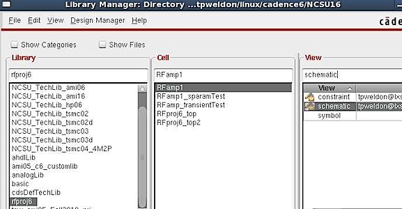
- Creating a layout for your RF amp
- Open your RFamp1 schematic as follows
- Make sure that none of your pins have names that could
interfere with global names/variables.
- NEVER name a pin "gnd" or "vdd" or
"vcc" or "vss"
- NEVER NEVER NEVER use "gnd" pins
anywhere except in the top-level schematic
- Check the schematic in Schematic-XL tool using
MenuBar::Check::CurrentCellView (yellow arrow below) and make
sure no errors are reported in the CIF window
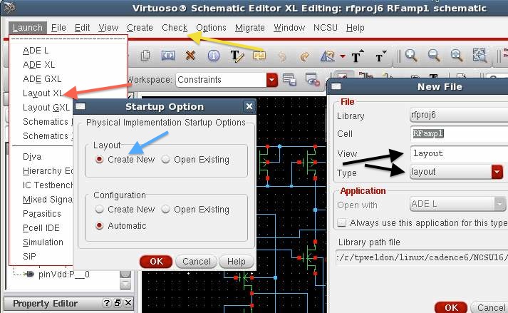
- As shown below, launch the Layout XL tool (red arrow below)
- In the popup window, select create new (blue arrow below)
- In the next popup make sure layout is the view type (black
arrows below)
- Print out your new schematic with a
white background. ( P6 )
- The layout window should now appear beside the schematic
window
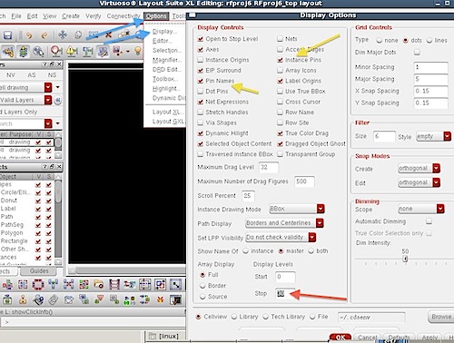
- As shown earlier above, in Layout XL, use
MenuBar::Options::Display to set the "Display Levels" to 0 to
30, and to set the check buttons "on" for "Pin Names" and
"Instance Pins." (reduced-size picture below)
- Then, Activate the annotation bowser pane in the layout
window using MenuBar::Window::Assistants::AnnotationBrowser
- Use MenuBar::Connectivity::Nets::ShowAllIncompleteNets to
see the "flylines" indicating the nets that must be connected,
(flylines will appear after components are placed in the
layout)
- This is a better way to do layout than
the "generateAll" method used to place items in layout
earlier:
- Select the transistors only in
the schematic without
selecting any I/O pins in the schematic
- In Layout editor
MenuBar::Connectivity::GenerateSelectedFromSource (red
arrow below) to place transistors in the layout
- DO NOT use "AllFromSource"
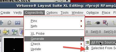
- Then, select each pin one at a time in the schematic, and
place them in the layout using
MenuBar::Connectivity::GenerateSelectedFromSource (yellow
arrows below)
- As in the example below, the pins are in the same relative
locations as in the schematic. pingnd on bottom,
pinvdd on top, inputs on left, outputs on right (4 yellow
arrows below)
- Your layout after pin placement should look like the
layout below
- If you dont see the flylines:
- Then, activate the annotation bowser pane in the layout
window using
MenuBar::Window::Assistants::AnnotationBrowser
- Use MenuBar::Connectivity::Nets::ShowAllIncompleteNets
to see the "flylines" indicating the nets that must be
connected, as illustrated below
- To get flylines to work, you must
activate the annotation browser pane in the
layout window using
MenuBar::Window::Assistants::AnnotationBrowser
- Flylines indicate where incomplete connections exist
that have not yet been be wired by you
- The foregoing method of placing pins one at a time allows for much easier control of
pin placement than the Generate::AllFromSource "brute force
"method described in project05_s15supplementGenerateAllComponents.html
(hopefully you will never have to resort to "generateAll")
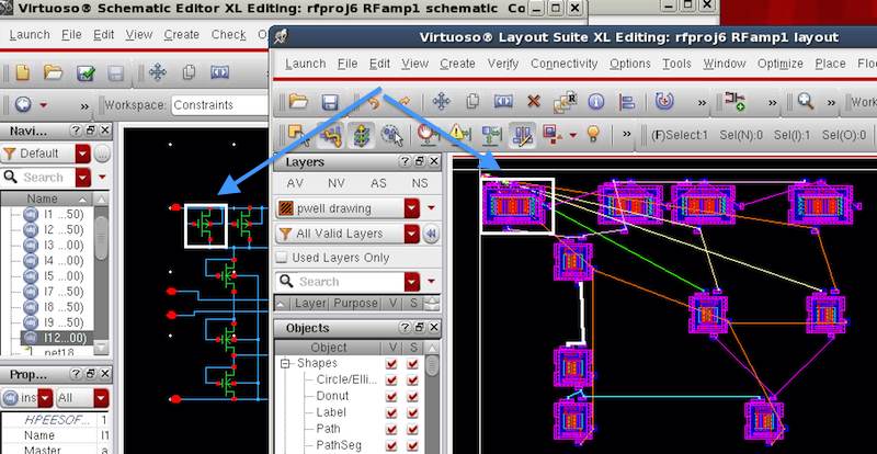
- If you click on a device or pin in the layout or schematic,
the corresponding item should also be highlighted
- Selecting a pin in the layout highlights a pin in the
schematic
- Selecting a transistor in the layout highlights a resistor
in the schematic (blue arrows below)
- Check for this, and if this
highlighting feature is not working, delete the layout
and start over!
- Save your layout now
- In your layout, you can move devices
by typing "m" in the layout area, clicking a device,
and moving the mouse (typically not
dragging, but click-and-move, the mouse on some systems)
- Select a device and type "q" to see
properties
- Move the transistors apart, so that there is enough room to
fit a few "wires" between each
- Once you have positioned your transistors, print out your
preliminary layout with a white
background with "flylines" of incomplete nets visible
as above . ( P7 )
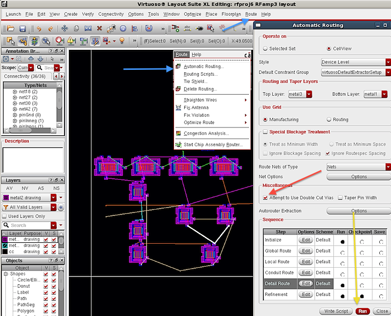
- Automatic routing
- Older versions of the software did not give access to the
autorouter, so all routing (wiring) had to be done manually
- The autorouter seems to now be
available!
- It does not seem to be working perfectly, but the autorouter
is WAY better than manual routing
- To use the autorouter, first select all of the devices in
your layout
- Then, MenuBar::Route::AutomaticRouting (blue arrows below)
- Select the "attempt use cut vias option" (red arrow below)
since this seems to avoid short circuits
- Hit Run (yellow arrow below)
- Hopefully, you will see much of your wiring appear
automatically
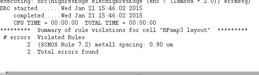
- Unfortunately you often get errors, ...so
- Immediately run DRC check
- Hopefully, you will only get a few errors that you can
easily correct by hand, such as below
- Correct the autorouter errors by hand
using the manual techniques below
- Another handy command for fixing errors can be
MenuBar::Edit::Basic::Chop to remove chunks of
metal. this is particularly handy for fixing
paths, where you usually dont want to delete the whole
path. To learn more, just invoke the
help-button when the chop popup appears.
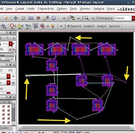
- When you finish autorouting, your layout will hopefully have
no DRC errors, will be mostly wired, and have only a few
remaining flylines as below
- Run DRC check
- If you have no errors, Save your
layout now!
- Fix any errors, and rerun RDC
- The remainder of the layout must now be done manually , as
described below
- Manual routing
- Use manual routing to complete the task of wiring your
circuit
- Try to only use metal1 and metal2 to wire your circuit
- Try to use metal1 vertically and metal2 horizontally, ... as
much as is reasonable. This helps prevent "roadblocks"
- Vias
- As you wire the circuit, sooner or later you will need to
cross over a wire by jumping up to a higher metal
layer. to do this, you need to use a via to connect
between layers
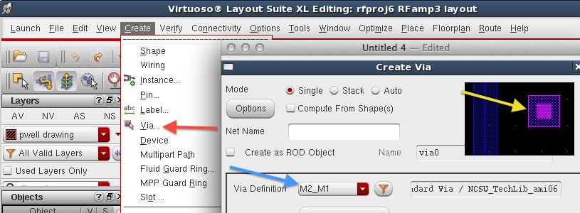
- To connect from metal1 to metal2 use a via from
MenuBar::Create::Via (red arrow below) and select M2_M1 for
a via to connect from metal1 to metal2, and you should see a
via appear in your layout (yellow arrow below) that connects
metal1 (blue metal) to metal2 (magenta metal)
- Note: in cases where a wire conducts more than 1 mA of
current, use one contact per mA
- Beware of long wires! Note
that each metal has about 0.1 ohm/square and poly has about 25
ohm/square and each metal-metal contact is about 1 ohm
- Paths
- Select metal1 on the LayersPalette in the left side of the
Layout XL window (red arrow below), then type "p" when your
mouse is in the layout area to create a metal1
path. (Alternatively use
MeuBar::Create::Shape::Path)
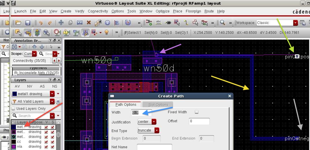
- As illustrated in the example below, to draw a path:
- first select metal1 or metal2 to select the metal layer
to draw your path (red arrow below)
- Make sure the createpath popup has the right path
thickness (0.9 is minimum for metal1 and metal2)
- Draw the path (yellow arrow below) from the output pin
(gray arrow below) to the wn50 drain (purple arrow below)
- Also shown is an unconnected pin and flyline (green
arrow below)
- Rectangles
- Experiment with typing "r" in the layout area to draw a
metal1 rectangle
- Connect all the devices, and dont
forget to DRC check and save every 5 minutes!
- Connect your circuit as illustrated above using metal1
paths, and using flylines as guides of where connections are
needed
- Experiment with typing "r" in the layout area to draw a
metal1 rectangle
- Print out your final RFamp layout as below, except with a white background, fully
wired, passing DRC, and LVS. (
P8 )
- It must pass BOTH DRC and LVS
- When you finish wiring the layout, run DRC (design rule
check) using MenuBar::Verify::DRC as shown below
- Make sure no errors are present by inspecting the message in
the CIW window (red arrow below)
- For a list of rules see MOSIS.com
ON Semiconductor C5N SCMOS_SUBM
rules
- Take a snapshot of your CIW output for DRC showing "Total
errors found: 0" as above. ( P9 )
- When you finish DRC, run extraction (extract schematic from
layout) using MenuBar::Verify::Extract as shown below
- Make sure no errors are present again by inspecting the
message in the CIW window (red arrow below)
- When you finish extraction, run LVS (layout versus
schematic) using MenuBar::Verify::LVS as shown below
- Use the "form contents" option (green arrow below)
- Use the browse buttons (yellow arrows below) to navigate to
the schematic view and extracted views of your design
- Check that the proper files and views are loaded into the
form (red arrows below)
- Make sure no errors are present again by inspecting the
message in the CIW window to see the message "netlists match"
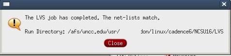
- If your design layout matches your schematic, you should get
a netlist match popup as follows
- UNTIL YOU SEE THE FOLLOWING
MESSAGE, YOUR DESIGN IS INCORRECT!
- Repeat the DRC, extract, and LVS steps on revisions of your
design until you get the above message
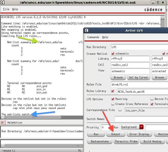
- The LVS output file often has good information for debugging
errors
- You should always check the output
file, as below, even if you get the "netlists match" popup
- To access the LVS output file, click the output button (red
arrow below)
- Take a snapshot of your LVS output window as shown above
showing "the netlists match" as above for your RFamp1
layout. MAKE SURE that you include the full output up
through the "netlists match" line (blue arrow above), and
include the full file name of your design (green arrow above)
( P10 )
- Final Top-Level Schematic and layout
- Save your work and close all
layout, schematic, symbol windows
- NEVER NEVER NEVER use "gnd" pins
anywhere except in the top-level schematic
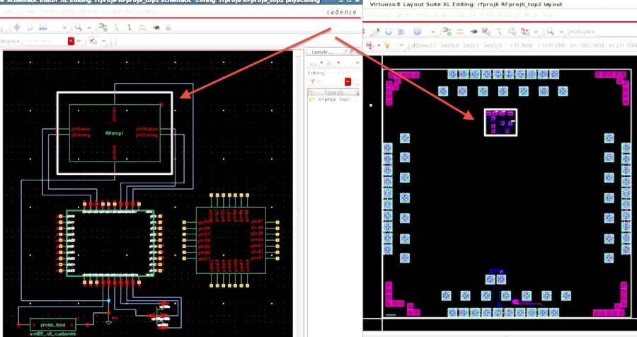
- Now that you have created your RFamp symbol, schematic, and
layout, you can use it in your top-level padframe schematic
- Open your top-level schematic that has the padframe from
Library Manager window
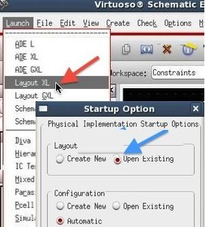
- Open the layout view from the schematic using
MenuBar::Launch:layoutXL "open existing" as below
- In schematic editor, use MenuBar::Create::Instance and
select rfproj6/RFamp1 and place it on your schematic and wire
it as follows
- As before, select the new symbol of the RFamp in the
schematic
- Go to the layoutXL window and use
MenuBar::Connectivity::GenerateSelectedFromSource to place
your new cell in the layout as follows
- Make sure connectivity is retained such that the highlighted
symbol in the schematic results in the highlight of the
corresponding cell in layout (red arrows below)
- Wire everything up as before
- Save your work
- Repeat the DRC, extract, and LVS steps on revisions of your
design until you get the "netlists
match" message
- The LVS output file often has good information for debugging
errors
- You should always check the LVS output
file, even if you get the "netlists match" popup
- Take a snapshot of your top-level-with-padframe final layout
with a white background with
everything in the padframe as shown above, but fully wired. ( P11 )
- Take a snapshot of your top-level-with-padframe CIW output
for DRC showing "Total errors found: 0". ( P12 )
- Take a snapshot of your top-level-with-padframe LVS output
window showing "the netlists match". MAKE SURE that you
include the full output up through the "netlists match" line,
and including the full file name of your design as before ( P13 )
- Save your work
- In class, show the instructor
that:
- 1) DRC has no errors,
and "netlists
match" for RFamp and ( Q1 ),( Q2 )
- 2) DRC has no errors,
and "netlists
match" for Top-Level design with
padframe.,( Q3 ),( Q4 )
- Save your work
- Exit the program, File->Exit
Report
NOTE ReportTemplate: Use the Project Report Template
and keep answers to questions on
consecutive sheets of paper with all plots at the end.
Do not add extraneous pages or put explanations on separate
pages unless specifically directed to do so. The instructor will
not read extraneous pages!
Only turn in requested plots (Pxx )
and requested answers to questions (Qxx ).
All plots must be labeled P1, P2, etc. and all questions must be
numbered Q1, Q2, etc. YOU MUST ADD CAPTIONS AND FIGURE
NUMBERS TO ALL FIGURES!!
Copyright 2010-2015 T. Weldon
Cadence, Spectre and Virtuoso are registered trademarks of
Cadence Design Systems, Inc., 2655 Seely Avenue, San Jose, CA
95134. Agilent and ADS are registered trademarks of Agilent
Technologies, Inc.