Microwave Circuits and
Metamaterials
Project 1
Overview
First, form project groups for the
semester.
The objective of the tutorial is to become familiar with the basics
of Agilent ADS software and Cadence software, and pulse reflections.
NOTE: Use the Project Report Template and keep
answers to questions on consecutive sheets of paper with all plots
at the end.
To save considerable time and effort,
look at the template before doing any work, and copy/paste
data into your template as you complete the projects.
IN NO CASE may code or files be exchanged between students, and
each student must answer the questions themselves and do their own
plots, NO COPYING of any sort! Nevertheless, students are
encouraged to collaborate in the lab session.
Only turn in requested plots (Pxx )
and requested answers to questions (Qxx ).
Part 1
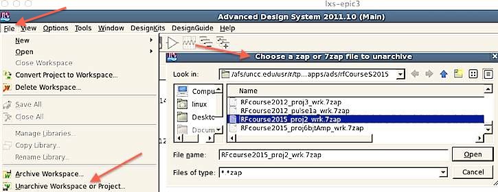
Start the software:
- Download the 7zap archive RFcourse2012_pulse1a_wrk.7zap
to your ~/apps/ads directory
- Use MenuBar::File::Unarchive to extract the project into
your ADS directory as follows
Move the zip-file into the apps/ads directory, and extract
it
You should find a new directory RFcourse2012_pulse1a_wrk
created in apps/ads
Run ADS and open the new RFcourse2012_pulse1a_wrk workbook
by double-clicking it
Go down through the directory tree to pulse1/schematic and
double click that design file. Double-click the schematic in
the right half of the window, and the following schematic
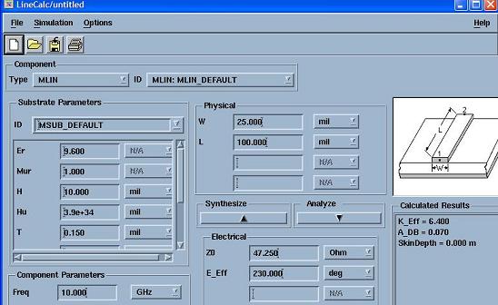
should appear. (1 mil = 1/1000 inch)
Save a snapshot of the schematic and paste it into your
report. ( P1 )
- Make sure that your
plots, component
values,
legends, axes, and fonts are legible in your report!
- For snapshots use the
Linux menu Graphice::Ksnapshot and select the option
to take a legible snapshot of a window rather than full screen
Part 2
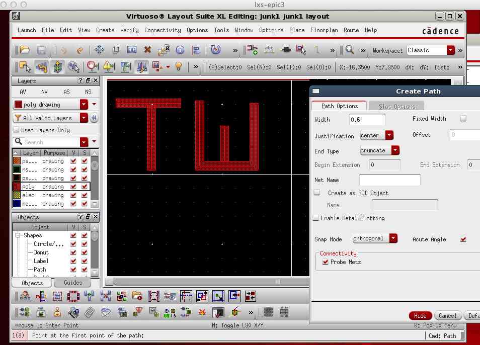
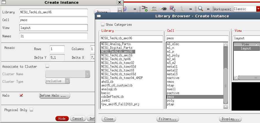
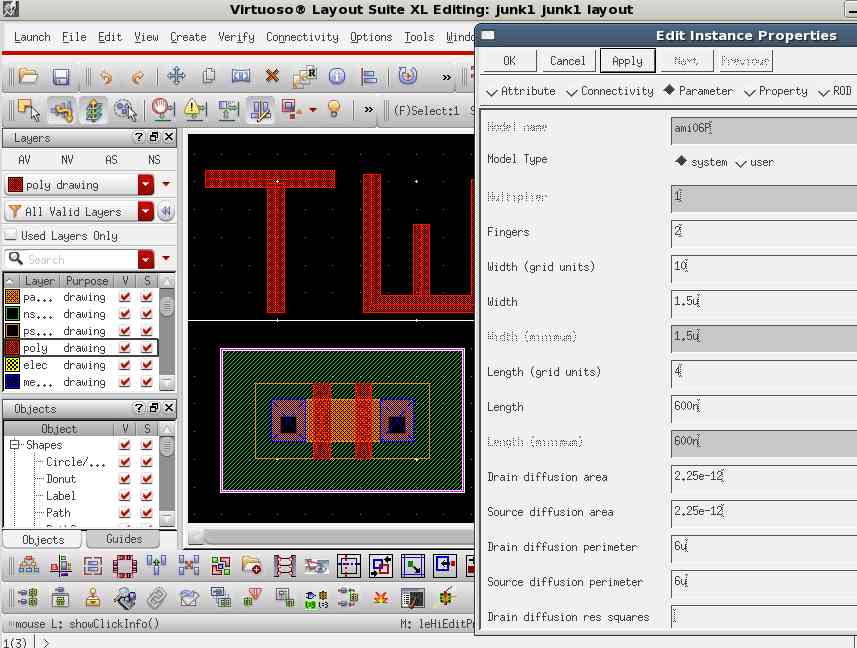
- Place the transistor near your initials as in the following
figure
- Using MenuBar::Edit::Basic::Properties select the transistor
and edit the transistor property (2-finger gate) as follows:
Part 3
NOTE ReportTemplate: Use the Project Report Template
and keep answers to questions on
consecutive sheets of paper with all plots at the end.