EEGR6437, Mixed Signal IC Design Project 2
Note:
Please form groups of 2 or 3 for this project (ideally
the same group for final project). Note: students in
6000 sections should group together.
Overview
The objective of the project is to design a simple
R2R ladder Digital to Analog Converter (DAC).
The R2R DAC you are given is not the best design!
(It has many problems.)
IN NO CASE may
code or files be exchanged between groups,
and each group must answer
the questions themselves, NO COPYING!
Turn in all requested plots ( Px ).
Place answers to all questions
( Qx ) on a separate sheet of paper,
with questions consequitively numbered.
Keep answers to questions only 2 or 3 sentences long,
or 2 or 3 lines of computation, in most cases.
2 or 3 sentences should
suffice for most explanations.
Only turn in requested plots ( Pxx )
and requested answers to questions ( Qxx ).
Part 1
BEFORE DOING ANYTHING!!
This project is done in AMI 0.5 micron, so you must
run the proper startup scripts.
See the instructions on the course website.
Part 2
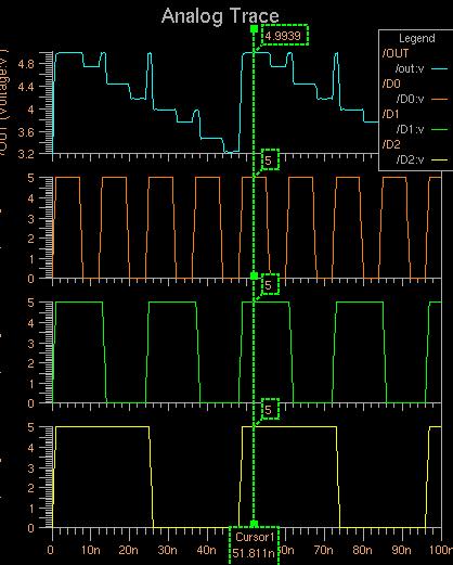
Do a time domain Accusim simulation and apply
appropriate digital inputs (D0-D2) to
ramp the DAC through all 8 states, starting at logic 111
and decreasing until logic 000, as shown below.
The voltage steps at the DAC output
should occur every 6 nanoseconds,
and the duration of the simulation should be 100 ns,
as illustrated below. Use 0.1 nS rise and fall times on the
edges of the input waveforms.

Plot the input voltages (D0, D1, D2 )
and output voltages and turn this in.
( P4 )
What are the output voltages at
D2,D1,D0 = logic 000 and 111? (Use the cursor in Accusim to measure
voltages accurately)
( Q2 )
Make a table of the 8 output voltages for all
possible inputs
(logic level inputs, i.e., 000, 001, 010, etc.),
AND measure the voltage step sizes
from one level to the next. Turn this in.
( Q3 )
Are the stepsizes uniform? ( Q4 )
What is the +/- accuracy of the DAC in LSB,
assuming that:
LSB = (Vmaxout - Vminout)/(8 - 1)?
( Q5 )
Tabulate the 3 stepsizes, 000 to 001, 000 to 010,
and 000 to 100, and include the ratio
of each stepsize to the next smaller one.
(Ideally, the ratio should be 2.) Turn in this table.
( Q6 )
What is causing the "glitches" in the output?
( Q7 )
Search the web for "de-glitchers" for DACs , not for ADCs.
Analog Devices, Inc. is usually a good place to look.
Explain the
underlying mechanism, in terms of the circuit,
that causes these glitches.
(Hint: do the glitches tend to occur at particular
bit transitions and are they larger at particular
transitions and is the timing perfect,
and what added circuits might prevent glitches?
Are there timing problems?)
Part 3
Do a time domain Accusim simulation and apply
appropriate digital inputs (D0-D2) to
step the the DAC from D2,D1,D0 = logic 000 to logic 100, and back to 000.
This is exercising the MSB of the DAC.
The steps should last for at least 10 nanoseconds,
and you must use 0.1 ns risetime.
Use a small enough time window (20 ns simulation stop time)
to clearly see the
rise/fall time of the output pulse. For this simulation:
Plot the input voltages (D0, D1, D2) and output voltages and turn this in. ( P5 )
What is the rise/fall time of the DAC to within 1/2 LSB of
final value?
(also, note any time delay in addition to rise/fall time of the edges)
( Q8 )
Based on the previous question,
what would you estimate the maximum DAC speed to be? (samples/second)
( Q8b )
Use the create-sdl method as mentioned in the
AMI 0.5 micron notes to do the following layout.
(Run IC Station, and use the "Create-SDL" pallette command, and select
the SDL viewpoint as the schematic source.)
DO NOT USE OTHER METHODS PREVIOUSLY GIVEN IN THE
MANUALS OR PROJECTS. Place all of your components before you place
your ports. Create-sdl is the ONLY WAY to place your ports.
You must initially create the cell with "Create-SDL",
you cant start some other way
and hope to "clean it up." It is hopeless and you
will lose all of your layout ...
Do a VERY ROUGH layout of the DAC (basically
just pace the parts, then place the ports, and autoroute
and compress them). Do not get bogged down, just work quickly
to get a rough estimate of size. (If you have extra time try
using DRC and cleaning up the layout for practice.)
Just make sure all the parts
get placed, and do one pass of autoroute. Place the layout in a
padframe and turn this in. This part of the project
is just to estimate the rough size of the DAC, as you
would if it was being used in some larger design.
also,
before placing ports, unselect everything in the
schematic, then click place-port. (or select one port
at a time and place it, but dont select ports plus schematic parts
at the same time )
Turn in your layout,
inside a padframe so the size can be judged.
(For this quick layout,
ont worry if the pads dont place and you only get corner pads and
green lines)
( P6 )
Part 4
In this final part, you will go through the COMPLETE procedure of layout
for a ridiculously simple cascade of 3 inverters.
Create a schematic of a 3-inverter AMI 0.5 micron cascade,
where the first inverter is minimum size,
and each successive stage is twice as big.
(This is how you would design a buffer to drive a pin.
DO NOT FORGET TO DO THIS IN YOUR FINAL PROJECT!)
Exactly follow the recipe given in the
AMI 0.5 micron notes to do a full layout with schematics,
SDL-layout, LVS, and DRC on the whole chip,
INCLUDING PADFRAME. DO NOT USE OTHER METHODS PREVIOUSLY GIVEN IN THE
MANUALS OR PROJECTS. Create-sdl is the ONLY WAY to place your ports.
You must begin with this, you cant start some other way
and hope to "clean it up." It is hopeless and you
will lose all of your layout ...
any deviation from the known recipe for success almost guarantees failure ...
so use the exact procedure as given in the AMI 0.5 notes
Note, you MUST add filler. Filler is necessary in sub-micron process
because they polish the substrate between steps of
fabrication. The filler prevents "low-spots"
or polishing through to the next layer.
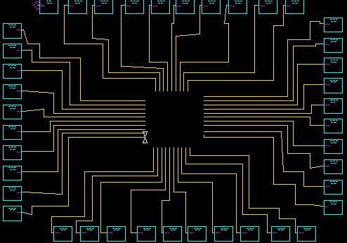
To save time, I have a top-level schematic for
the 40 pins of a chip in ~/tpweldon/pub/mixsigxx/project2 .
It looks like this:
 For the 3-inverter layout, turn in:
Top-level schematic with pads.( P7 )
Top-level layout with pads.( P8 )
Main schematic (without pads).( P9 )
Symbol for your main schematic.( P10 )
Layout corresponding to your main schematic.( P11 )
Part 5
There are other intersting examples on the system.
Look at the 1.2 micron DAC schematic and layout. (Under "Speceal" parts
in the SDL libraries menu of design architect.)
How many bits is the DAC?( Q9 )
What is the size of the DAC in microns?
(Be careful, .... are you using 0.5 or 1.2 micron startup script.)
( Q10 )
Look at the diffamp1u05 ami 0.5 diffamp. In the layout,
spot the ground ring that solidly contacts the substrate all the
way around the amplifier.
How many ground contacts are inthe ground ring?( Q11 )
Is there filler in the amp?( Q12 )
What is the size of the amp (microns x microns)( Q13 )
Look at the capacitors available (near the easyfets) and see how they
are constructed in the layout.
What layers comprise the top and bottom
plates?( Q14 )
How many square microns is the area of the AMI 0.5 micron,
.125 pF capacitor?( Q15 )
Report
Write any comments or observations you may have
directly on the printouts. Type or clearly handwrite.
Do not add extraneous pages or put explanations on separate pages
unless
specifically directed to do so. The instructor will read
extraneous pages!
Turn in a separate sheet with answers to all of the specific questions above.
Write a cover sheet plus a 1-page double-spaced summary of the project.
Stick to discussion of the results you observed.
Include any problems or unresolved issues in the summary.
Turn in all requested plots ( Px ).
Place answers to all questions
( Qx ) on a separate sheet of paper,
with questions consequitively numbered.
Keep answers to questions only 2 or 3 sentences long,
or 2 or 3 lines of computation, in most cases.
2 or 3 sentences should
suffice for most explanations.
All plots must be labeled P1, P2, etc.
and all questions must be numbered Q1, Q2, etc.
Only turn in requested plots ( Pxx )
and requested answers to questions ( Qxx ).

