EEGR6437, Mixed Signal IC Design Project 1


Note:

Please form groups of 2 or 3 for this project (ideally the same group for final project). Note: students in 6000 sections should group together.

Overview

The objective of the project is to design a BJT/FET circuit that incorporates some of the most basic analog building blocks.

IN NO CASE may code or files be exchanged between groups, and each group must answer the questions themselves, NO COPYING!

Turn in all requested plots ( Px ). Place answers to all questions ( Qx ) on a separate sheet of paper, with questions consequitively numbered. Keep answers to questions only 2 or 3 sentences long, or 2 or 3 lines of computation, in most cases. 2 or 3 sentences should suffice for most explanations.

Only turn in requested plots ( Pxx ) and requested answers to questions ( Qxx ).

BEFORE DOING ANYTHING!!

This project is done in AMI 1.2/1.5 micron, so you must run the proper startup scripts. See the instructions on the course website.


Part 1

  • A.

  • Use Design Manager to copy the schematic for the circuit from ~tpweldon/pub/mixsigxx/project1/bjtdiff (~tpweldon/pub = /afs/uncc.edu/usr/r/tpweldon/pub ) where xx is this year. Make sure your copy of the circuit is copied properly, and is loadable by Design Architect.
  • Run an AC frequency sweep analysis (FREQ MODE). Dont forget to load your 1.2 micron spice models (File->Auxiliary). First select frequency sweep mode in accusim, add a 1 volt ac source (ADD FORCE) at input, and add traces to display the input and output. See the AC sweep section in the "Intro to Mentor" manual.
  • Print out the schematic, view the spice output file (Reports:ViewOutfile) and write (by hand) all DC currents and voltages on the schematic. ( P1 )

  • Plot the magnitude of the frequency response (i.e., the ratio of the output to input signals) in dB from 1 KHz to 1 GHz using logarithmic scaling of the frequency axis. (Use Results->Chart-ChartResults, and select dB magnitude). ( P2 )

  • Change R5 .
    Close the current simulation. Create a new copy of the schematic and change R5 to 10000 Ohms. Use MenuBar-->Libraries-->MGCAnalog then Palette-->Generic-->Resist-H to select the "normal/primitive resistor" from the Mentor built-in analog libraries.

  • For this new schematic with R changed, plot the magnitude of the frequency response (i.e., the ratio of the output to input signals) in dB from 1 KHz to 1 GHz using logarithmic scaling of the frequency axis. ( P3 )

  • With the change to R5, what are the collector currents in Q5 and Q6 and what are the voltages on the bases of these 2 BJT's?
    (use Report->ViewOutfile)
    Did they change? Explain why the gain went down in terms of gm x RL. Which one (gm or RL) changed the most? (also give IB, IC, GM and DC Beta for both transistors, Q5 and Q6) ( Q1 )

    Also, you can display some values on the accusim schematic by selecting a node and using the pull down menu (right-click) Add->FlagMonitor->Selected. (Be careful that you are sure that this displays initial, DC, transient, or final node voltage or current)

  • Change R5 back to its original value.
    On a separate sheet of paper, answer the following:
  • What is the role of Q4 in the circuit?. ( Q2)

  • What is the role of Q5 and Q6 in the circuit?. ( Q3)

  • What is the role of M1 and M2 in the circuit?. What is Rds and GDS for M2? ( Q4)

  • What is the role of Q1 and Q2 in the circuit?. ( Q5)

  • What is the role of C1 with regard to isolating the input signal from the second differential input? ( Q6)

  • Change R5 back to its original value, if you have not already done so.
    Perform a DC sweep analysis on the amplifier (remove the input/output capacitors if you need to).
    Plot the DC sweep . ( P4 )

  • Plot the derivative of DC sweep. Unselect all signals in the chart; use MenuBar-->Results-->WFCalculator; make sure Y is shown in the upper left since you want to operate on the Yaxis variable; click d/dt in popup; click WF; select the signal from the list; and click the upper right graph-key to plot a new chart.

    Be sure to use fine voltage stepsizes in the DC sweep, so you dont miss the correct peak value of the derivative. Keep decreasing stepsizes until you observe no change in the result. ( P5 )

  • Why does the peak derivative equal the AC sweep gain? ( Q7 )

  • Plot the input impedance as a function of frequency from 1KHz to 1GHz. To do this use the function Results:Chart:A/B to plot the ratio of input voltage divided by input current. Use a Log scale frequency axis LINEAR scale for the impedance axis and plot both magnitude and phase. ( P6 )

  • Do a time domain simulation and apply a 100KHz sine wave to the input. Increase the amplitude until the output voltage begins to clip. Plot the input and output voltages (plot the output at the "other side" of the output capacitor, where you can see the DC bias levels of the output). Dont "over-drive" the amplifier, drive it hard enough that only one "side" clips. ( P7 ) On this plot, what is causing the voltage to clip? Indicate the mechanism and transistors/devices involved. ( Q8 )


  • Part 2

  • Modify the original circuit by replacing the BJT differential pair with an 2 Lambda long x 1000 Lambda wide NMOS differntial pair. Print out the new schematic. ( P8 )


    What is the transconductance of the MOSFETS in the differential pair? ( Q9)

  • Plot the magnitude of the frequency response (i.e., the ratio of the output to input signals) in dB from 1 KHz to 1 GHz using logarithmic scaling of the frequency axis. ( P9 )

  • Compute the expected low-frequency gain for the NMOS diff. pair amplifier design, based on the trandconductances of the differential pair and the output impedances of the active loads and the differential pair devices. (Use Report:viewoutfile to see gm and gds, and make sure your devices are in saturation) ( Q10 )

  • Plot the magnitude of the frequency response with linear Y-axis (not in dB) from 1 KHz to 1 GHz using logarithmic scaling of the frequency axis. ( P10 )

  • . Perform a DC sweep analysis on the amplifier (remove the input/output capacitors if you need to). Plot the DC sweep . ( P11 )

  • Plot the derivative of DC sweep. Be sure to use fine voltage stepsizes in the DC sweep, so you dont miss the correct peak value of the derivative. ( P12 )

  • Does the peak derivative equal the AC sweep gain? ( Q11 )

  • Use ICStation to create a layout for both the original BJT-based and the FET differntial pair. (no need to layout the rest of the amplifier, just layout the two BJT's and 2 FETS in the two different differential amps) Put both of these layouts in a single layout cell, and print it out. If a fet in your circuit is wider than 100 microns, lay it out as several 100 micron wide fets in parallel. Alternatively, fold the fets by first carefully selecting the poly gate pins and then Palette-->DLADevice-->Edit-->Fold and enter 10 or some other number that results in a width of less than 100 microns. Remeber, lambda is 0.6 microns for the AMI1.2 process. ( P13 )

  • What is the approximate area in microns of the BJT differential pair? ( Q11 )

  • What is the approximate area in microns of the FET differential pair? ( Q12 )


  • Part 3

  • Use ICStation to create a layout for the original BJT-based amplifier. Start with a copy of the original schematic and replace the input and output capacitors by wires, and delete the third capacitor. (In essence, the end-user of your chip would place these capacitors external to your circuit.)

    Layout the whole amplifier, without a padframe. This layout will be a "rough layout," so you do not need to eliminate all DRC errors or all overflows.

    Fold the two fets by first carefully selecting the two poly gate pins and then Palette-->DLADevice-->Edit-->Fold and enter 8.

    On the folded FETS, make one source and drain and gate contact (for this rough layout do not bother to connect all the drains together, sources together, and gates together).

    Autoroute your layout, leaving a few overflows in the FETs. (You would need to complete all of the routing if this was a design going to fabrication).

    Use compaction to shrink the layout, and check it with DRC (design rule check). To get the compactiobn menu, leave the ADK Palette by clicking "Top" and then select the "Place and Route" Palette. Click "Compact" and use the "Box" tool to restrict compaction to the desired area of your circuit. Compact in the UP/Down/Right/Left as needed. Make sure to run DRC to see any errors induced by compaction. (Run DRC outsidce the region where BJTs are to avoid the BJT errors.) Print the layout.

    Note: AMI 1.2 micron process DRC may not be completely functional, since it may not recognize BJT's properly. ( P14 )

  • LVS (Layout Versus Schematic):
    run IcTrace(M) to do LVS and see the report. Anything other than a smiley face is no good. Use a schematic with all the grounds connected together for the schematic (and use the lvs viewpoint as the source file for comparison!)
    Note: AMI 1.2 micron process LVS is not completely functional, since it does not recognize resistors properly.
  • Create a padframe with ADK->padframe->1.2micron. Note: you must have the schematic open to do this, otherwise you only get 4 corner pads plus green lines.

  • Position the amplifier near one of the corner ground pins of the padframe.

    Only AFTER you finish ALL connections in the circuit: Use "Object->Add Overflow" to add overflows to connect the amplifier input and output to analog pins on the padframe. You must be very careful to "hit the right spot" on the analog pin.

    To add overflows you must enter connectivity edit mode (CE) by the command Context:SetCellConfig:ConnectEdit, then add overflows as Object:Add:Overflow.

    Also add overflows connecting the amplifier ground pin to the padframe ground pin. Connect the amplifier power using a overflow to another analog ground pin. The padframe power supply may be too noisy for an anolog circuit, if there are digital circuits on-chip. Use the autorouter to route the 4 overflows created above.

    Finally, add a metal-1 strap to short out one of the resistors built into the analog pad connected to the amplifier power supply. Print the layout. ( P15 )
    Reset IC station to Correct by Construction editing mode by using: Context:SetCellConfig:CorrectbyConstruction

    Note: do not "connect by hand," always route using overflows and the autorouter. 90% of bad chips are do to errors when routing/connecting "by hand."

  • Create a gds-II tapeout of the layout with MenuBar-->Translate-->WriteGDSII naming your cell whatever.gds.

    To check that your GDSII was written properly, close all Mentor tools. Then open a new ICstation and run MenuBar-->Translate-->ReadGDSII to check the file. Show your GDS-II layout to the instructor and have him sign the layout that was printed out, verifying that a GDS-II tapeout was completed. ( Q13 )


    Part 4

  • In this part, you will design a small SRAM.
  • Do not waste time. As quickly and efficiently as possible get the design working. Make good use of input signals instead of designing extra circuits.

  • Note: I have placed some very handy parts on the Design Architect palette menu under "Specials" right below the "EasyFets." I have provided a 3-bit decoder and a bank (1column X 8rows) of SRAM and a sense amplifier as new components. So you will only need to concentrate on the architecture, and adding the read/write decoder, timing circuits, and a tri-state driver for writing to bit/bitbar, etc.
  • Note: do NOT use any digital logic gates from the ADK library, where needed create your own gates from easyfets.
  • Place a decoder, sramcell, senseamp, and 8xcell sram column on a schematic in Design Architect. Open the schematics of these parts by selecting the symbol of the part, then right-click the mouse and OpenDown:Schematic. Print out the schematics of the four components. ( P 16,17,18a, 18b )

    The decoder follows the general design in Figs. 17.12 and 17.13. The SRAM cell follows Fig. 17.2. What happens to the decoder outputs (D0-D7) when the enable line is low? ( Q14 )

  • Please watch out for time-delay problems through the devices (especially decoder). These will cause synchronization problems between the decoder and SRAM cell data and sense amp timing. You may either adjust your external signal timing to account for these delay mismatches, or add circuits.
  • Design a 32-bit memory as an 8 rows by 4 columns array of the SRAM cells shown in Fig. 17.2 on page 332, where all devices are constructed using minimum size easy-fets. The overall architecture of your memory chip is shown in Fig. 17.11 on page 341, where n=3 and m=2, since we have 8 rows and 4 columns. Use the decoders of Fig. 17.12 (the decoders and memory columns are given to you, DONT DESIGN THESE!).

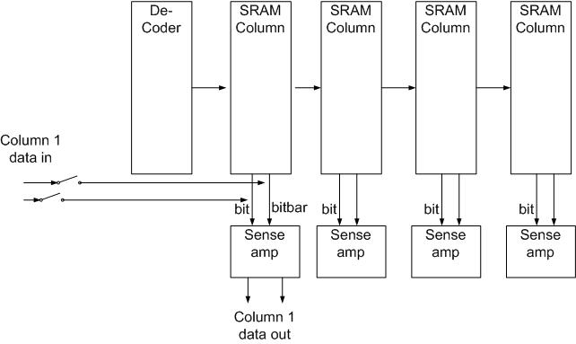
    A rough block diagram would be:

    where two switches (see later) are used to disengage the data in lines during read operations. Output data during read is taken directly from the sense amps.

  • The inputs to your memory are :
  • Address lines: A0 (LSB) to A2 (MSB most significant bit)
  • Write: read=low, write=high
  • Tri-state (or more simply, the switches shown on the input data): High isolates the input data bus from the SRAM
  • Clock: Low during first half of the read and write cycles, high during second half; assume a 100 nS clock period
  • You should organize the memory timing as follows:

  • Address, read-write, and tristate (inputs) change synchronous with clock falling edge
  • During a write cycle (read=low)
  • During the whole cycle, sense amplifiers are disabled, and the data bus is configured as input data coming into the chip to drive the BIT and BITBAR data lines of the SRAM
  • During the whole cycle, the row in SRAM corresponding to the address of the memory word being written is selected/enabled
  • During a read cycle (read=high)
  • During first half cycle, sense amplifiers are outputting data from the prior cycle, the bit and bitbar lines are precharged to near Vdd, and the data bus is configured as output from the chip
  • During the second half of the cycle, the precharge is disengaged, the decoder is enabled and selects the sram cell, the sense amplifiers are turned off and pre-charged by the sram cell data, and as soon as the next cycle begins the stored charge determines the output data (see below and the senseamp schematic for more detail)
  • For sense amplifiers, the timing of a read cycle is:

    
                                    _____ Data is ready here
                                   |
                                   v
                            ______                    
    clock           |______|      |    
                            ______                          
    prechargebar    |______|      |
                     ______                                 
    sense           |      |______|
                            ______                          
    decoder enable  |______|      |


    In the first half cycle:
    When prechargebar is low, bit and bitbar are pulled high, precharging both bit and bitbar to a high voltage while the sram cells are disabled because the decoder enable is held low. At the same time, the sense line is high, turning off any connection between the senseamp and bit or bitbar. Also, the bottom transistor in the senseamp is on, so the senseamp is on, and the data out (dat) is from the prior cycle.

    in the second half cycle:
    The prechargebar goes low, disconnecting the precharge of bit/bitbar, and the decoder is enabled to dump the ram contents onto the bit/bitbar lines. At the same time the sense line causes thesense amp bottom transistor to turn off, and the series fets on bit and bitbar to be turned on. During this time the sram cell contents tend to charge/discharge bit/bitbar cusing a stored voltage difference inside the senseamp (which is turned off because of the bottom transistor).

    at the very end, when the senseamp goes high again, the stored charge internal to the senseamp from bit/bitbar determines the state of the data output (dat) for the following half-cycle.

    Note: do not use decoders at the sense amplifier outputs at the bottom of Figure 17.11 on page 341, in the Data selector/decoder. Assume that the system uses 4-bit-wide words, so you want all 4 bits as output (rather than demultiplexing with the Data selector/decoder at the bottom of Fig. 17.11).

    Do NOT use the amplifier in Fig. 17.10 of page 340 with minimum size easyfets (except the two precharge precharge devices should be 2x as wide).

    For precharge, use the methods of Figs 17.9 and 17.10.

    Include switches on the 4 data input pins, using the transmission gates of Fig. 13.1 on page 255, with devices 2x as wide as the smallest easy-fet. The use of these will allow you to more easily test your SRAM in Accusim. The switches isolate the the data inpput sources from the bit/bitbar lines during a read operation.

    For the write operations, the switch should be on and you drive the data ports with external voltage sources. For the read operation you can turn the switches off, effectively decoupling the voltage sources so you can monitor the internal workings of the chip to see if the data was indeed stored. For convenience, you MUST add input/output ports on both sides of the switches to your schematic, so it is easier to see these signals in accusim. Also, for convenience it is easiest to use separate input and output pins for the data (rather than a single bidirectional pin for input output).

    When you finish the design, print out a copy of your schematic, clearly labeling the required pins defined above. ( P19 )

    Show a simulation in accusim of successively writing and reading data "1111" and "0000" to memory addresses 000, and 001 ( P20 )


    Part 5

  • Use ICStation to create a layout for the complete SRAM including the row and column decoders, sense amplifiers, and tri-state data bus.

    But first: are your outputs suized properly to drive the pads?? See section 11.4 and assume your output pad is 5 pF. (Also see Weste and Eshraghian p. 219). What is the optimum sizing ratio in successive stages of a chain of buffers (what is A in Eq. 11.22) ? ( Q15 )

  • Create a new cell with a padframe. Copy the SRAM cell into the cell with the padframe. Position the SRAM near one of the corner ground pins of the padframe. You need not connect the SRAM signals to supply pins for this layout. Print the layout. ( P21 )

    Note: in general, do not "connect by hand," always route using overflows and the autorouter. 90% of bad chips are do to errors when routing/connecting "by hand."

    Use compaction to reduce size. Makes sure it passes DRC. (Compaction tends to crash, so save your work often!)

  • Create a gds-II tapeout of the layout. Show your gds-II layout and ICstation layout to the instructor and have him sign the layout that was printed out, verifying that a gds-II tapeout was completed, and the layout passes DRC. ( Q16 )


    Report

    Write any comments or observations you may have directly on the printouts. Type or clearly handwrite. Do not add extraneous pages or put explanations on separate pages unless specifically directed to do so. The instructor will not read extraneous pages!

    Only turn in requested plots ( Pxx ) and requestes answers to questions ( Qxx ). All plots must be labeled P1, P2, etc. and all questions must be numbered Q1, Q2, etc.

    Turn in a separate sheet with answers to all of the specific questions above.

    Turn in all requested plots ( Px ). Place answers to all questions ( Qx ) on a separate sheet of paper, with questions consequitively numbered. Keep answers to questions only 2 or 3 sentences long, or 2 or 3 lines of computation, in most cases. 2 or 3 sentences should suffice for most explanations. All plots must be labeled P1, P2, etc. and all questions must be numbered Q1, Q2, etc.

    Only turn in requested plots ( Pxx ) and requested answers to questions ( Qxx ).


    Copyright information