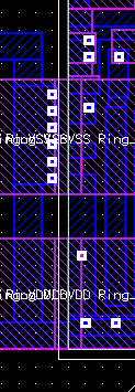
 Analog pad next to digital pad |
 Digital pad next to digital pad |
The difficulty seems to stem from the asymmetry of the digital pads. The following problems may not exist, depending which side of the digital IO pad the analog pad is placed against. In the unaltered 1.2 micron standard padframe, there are two places where analog and digital pads come together. The lefthand side of the padring seems not to have the VDD/VSS short-circuit problem, but the analog/digital pad on the right hand side does have this problem. Similar problems occur due to pad asymmetry in the 2.0 micron padframe.
It would be very nice to have symmetric pads.
Please email comments/suggestions/corrections.
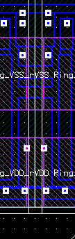
Email: tpweldon@uncc.eduIn the left image below, an area of Metal1 (the furthest left such area, in blue) runs between the two power rings. Under the lower power ring, the Metal1 of the left pad meets a Metal1 area of the right pad that is connected by VIAs to the lower power ring. The Metal1 of the left pad is also connected by VIAs to the upper power ring.
The problem does not appear on the digital-digital pad case shown on the right, since the Metal1 region has no VIAs connecting it to the upper power ring.
|
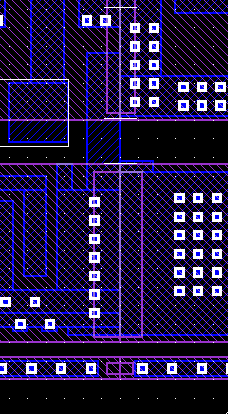
Analog pad next to digital pad |
Digital pad next to digital pad |
In the left image below, an area of Metal1 (in blue) runs between the two power rings. Under the upper power ring, the Metal1 of the left pad meets a Metal1 area of the right pad that is connected by VIAs to the upper power ring. The Metal1 of the left pad is also connected by VIAs to the lower power ring.
The problem does not appear on the digital-digital pad case shown on the right, since the Metal1 region has no VIAs connecting it to the upper power ring.
 Digital pad next to analog pad |
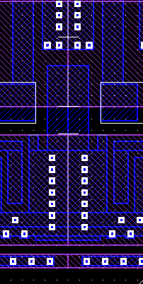 Digital pad next to digital pad |